A Look Behind the Mask of Multi-Patterning
By Michael White, Mentor Graphics
An overview to the mystery of Multi-Patterning
At the rate that new technology nodes keep racing by, it sure feels like we’re speeding down the Autobahn in a Ferrari, pedal to the floor. The first 16-/14-nm production designs for those fabless companies on the bleeding edge are already being released to production, with many more companies doing test chips. At the same time, 10-nm process development has peaked and begun winding down for the leading foundries, with 7-nm development already kicking off…
The commonality between 20/16/14 nm, 10 nm, and likely 7 nm is the need to use one form or another of multi-patterning (MP). Thus, it’s worthwhile to explore the various MP approaches, how they differ by technology node, and where the IC manufacturing/IP/EDA ecosystems are in the delivery of solutions.
The 20-nm technology node was the first that required an MP approach (double patterning, or DP) to image features. Although the 16-/14-nm node introduced a new transistor design (FinFET), the rest of the 20-nm back-end-of-line (BEOL) was maintained. Because 16-/14-nm didn’t materially change the BEOL pitches, the DP strategy also remained the same.
Things became far more interesting with 10 nm. The 10-nm node sees the continued use of DP for select layers, but also introduces triple patterning (TP), variants of quadruple patterning (QP), and variants of spacer-assisted double patterning (SADP). Let’s look at some of DP’s unique attributes, and then contrast that with the subsequent MP approaches.
Comparing and Contrasting MP Approaches
Multi-patterning became a necessity because next-generation extreme-ultraviolet (EUV) lithography tools were not yet ready for production, and the existing object linking and embedding (OLE) for process control (OPC) software solutions could not image the needed geometries on their own. The technique of splitting the layout into multiple masks allows us to relax the layout pitch back into a k1 value that can be imaged with existing OPC solutions. However, unlike OPC, which doesn’t require designer involvement, DP imposes new layout, physical verification, and debug requirements on designers.
Double Patterning
Litho-Etch-Litho-Etch (LELE) is the most common form of DP used at 20 nm. The LELE DP technique splits dense layouts that can’t be printed with a single exposure into two lower-density layout masks. The foundry then uses two separate exposure processes to form two coarser patterns, which are superimposed to form a single finer image on the actual wafer. Mask assignments (coloring) in LELE DP are based on spacing requirements—polygons that are closer than the minimum DP spacing must be assigned to different masks. Mask assignment can be performed automatically by a specialized MP tool like Calibre Multi-Patterning, or manually by the designer.
DP analysis engines process a layout to determine coloring in a very different way than traditional physical- verification (e.g., design rule checking) tools perform layout analysis. The drawn layout polygons are typically translated into a virtual graph (Fig. 1). This graph represents the drawn polygons that interact from a coloring perspective and must be assigned to opposite colors because they’re spaced at or inside the minimum single-mask spacing constraint. Wherever this spacing is violated (blue markers), the two polygons creating these spacing violations must be assigned opposite colors to be “DP legal.” The polygons in the layout are represented as nodes in the graph, while the spacing constraints are represented as edges. The nodes in the graph are then colored, starting with one arbitrary color choice, and then alternating colors thereafter. An error marker (red line) is generated for odd cycles of nodes that have no alternating coloring solution to make them DP-compliant.
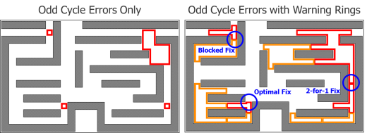
Among error markers, the ring error marker provides the most meaningful information for DP debugging (Fig. 2). This error marker identifies the polygons involved in an odd cycle that cannot be colored to be DP-compliant and that must be modified. In the figure, the ring marker communicates the entire cycle to the designer. The locations where the ring crosses the space between polygons represent the spacing interactions between those two polygons that connect the cycle at that point.
Each of the fix options in Figure 2 present different spacing changes. These will “break” the odd cycle and allow DP-compliant coloring assignments, removing the error. Any one of the fixes is equally valid from a coloring standpoint; therefore, designers are free to implement whichever one they prefer or best fits the layout. This type of error visualization greatly enhances design productivity.
However, fixing one odd cycle error can often lead to creation of another one that involves nearby polygons that weren’t part of the original error. To help designers avoid this time sink, Mentor’s Calibre Multi-Patterning provides an additional proprietary debug guidance, called a “warning ring,” for quicker resolution of odd cycle errors (Fig. 3).
The graph idea was also extended to help visualize issues associated with “anchoring” in DP design. With anchoring, the designer places markers on some polygons representing a preferred coloring assignment. Paths of interaction between anchored and unanchored polygons may form geometries that can’t be legally colored. These situations are visualized as anchor-path error markers (Fig. 4).
All of these innovations in DP error visualization help the designer understand and fix potential decomposition violations without even coloring the layout in the first place. This assistance enables “colorless” and “partially- colored” tapeout flows. Thus, designers can verify that the design is able to be legally colored, but leave the actual process of decomposing the layers into two colors to the foundry.
Triple Patterning
Use of 193-nm immersion lithography requires triple patterning (TP) to move polygon half pitches much below 64 nm. TP is analogous to DP, but divides the layout among three masks rather than two. Similar to DP, a virtual-graph approach is often used to analyze TP, but with an important difference. With DP, after coloring the first node of a graph, the next node must be the opposite color—toggling back and forth between mask 1 and mask 2 colors throughout the graph. With TP, after the first node is arbitrarily colored, the next node can be colored to either of the two remaining mask colors. With two coloring choices at each new node, the processing algorithm can backtrack and try another set of coloring choices if the first pass doesn’t produce a TP-legal coloring assignment (Fig. 5).
This approach is advantageous from a designer perspective, because the algorithm will be able to successfully color more of the design. As a result, the designer will need to resolve fewer coloring conflicts. However, computer scientists and mathematicians will recognize the computational repercussion. This new factor makes the general case of TP coloring a NP complete problem—resulting in exponential run times. Fortunately, EDA vendors have worked closely with the foundries to define a limited set of new TP-driven layout design rules to ensure more tractable computation.
With its more complex graphs, TP also creates the need for new types of error visualization. In addition to separators and other error markers between polygons that aren’t TP-compliant, Calibre supports specialized error markers for the most common TP error types. The first is referred to as a “K-4” (Fig. 6), showing four polygons (and their associated separators) involved in conflict. Moving any one of the polygons outside the single-mask spacing constraint resolves the coloring conflict for all four polygons.
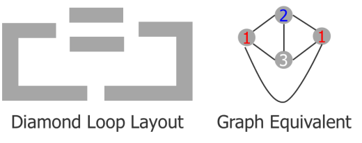
The second common layout and error configuration is a diamond loop equivalent (Fig. 7). The two “tips” in the graph have a minimum spacing constraint between them, requiring them to be different colors. However, they can’t be different colors due to the diamond equivalence construct, so this geometry can’t be legally colored. This diamond equivalent loop, in which the two tips interact with each other, now equals the four-polygon error type. If any one of the spacings indicated in the error marker is widened to meet the minimum same-mask spacing requirements, it resolves the error. The designer can choose from six spaces to increase to resolve this kind of error.
However, diamonds can connect to other diamonds to form long chains of diamond equivalences. If the ends of those equivalences ever have a minimum space requirement to each other, then there’s another error condition (Fig. 8).

This error visualization highlights the polygons “forced” to be equivalent. It also displays the diamonds driving the equivalence (shown by the hollow rings) and the spacing interaction between the interacting tips.
Quadruple Patterning
Quadruple patterning (QP), unsurprisingly, divides the layout between four masks. Like DP and TP, QP is typically analyzed using a virtual graph-based approach, and like TP, multiple potential coloring choices exist for each new node in the graph (three, instead of the two choices available with TP). Experience to date shows QP to be on the same order as TP from a computation perspective. It will be interesting to see if this holds with the creation of more 10-nm designs.
As was the case for TP, new error markers are being developed for the most common error types. For example, a “K-5” error marker represents the polygons and separators involved in a coloring problem where the five interacting polygons can’t be successfully colored with four colors (Fig. 9). Like the prior TP example, increasing the space of any one of the nine separators resolves the coloring conflict.
Self-Aligned Double Patterning
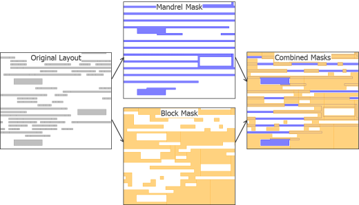
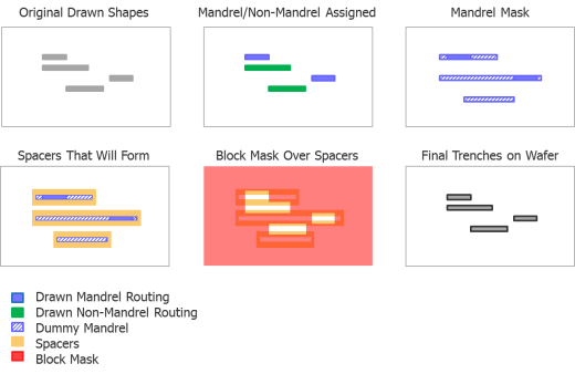
Self-aligned double patterning (SADP) represents a radical departure from the DP/TP/QP techniques. Like DP, SADP has two masks—the mandrel mask and block mask. However, these masks differ significantly from the masks usually found with LELE DP processes, both visually and functionally (Fig. 10).
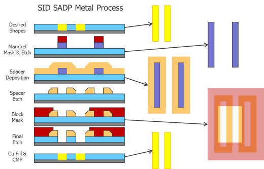
SADP uses a deposition and etch-step process to create spacers surrounding a patterned shape (Fig. 11). Spacer material is deposited on each side of the original shape, creating two shapes for every one shape originally defined, which essentially pitch splits the original lines. In the metal process application, the spacers define the gaps that will become dielectric material between the trenches targeted to be filled with copper to form the interconnect wires. Because these gaps between the wires will contain dielectric material, this form of SADP is called Spacer-is-Dielectric (SID). Figure 12 shows a representation of the SID SADP mask process.
Because it is so difficult to visualize how these two masks produce the drawn shapes on the wafer, debugging layout errors can be extremely challenging. With the arrival of new SADP processes also comes the realization that material mask and wafer manufacturing variability issues plague the complex dark field block mask.
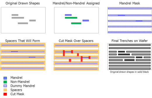
To mitigate these issues, we’re seeing the deployment of more regular layouts, and a simpler cut mask approach. Figure 13 shows the same layout from Figure 12, but uses an alternate mandrel-fill/cut-mask approach. The initial coloring assignment of the drawn shapes to mandrel and non-mandrel is the same. However, the masks are different. The mandrel mask shapes extend horizontally to the borders of the region being processed, creating a mask where the entire region looks like a diffraction grating of parallel lines—very lithography- friendly.
A cut mask with very regular cut shapes replaces the block mask used with SID SADP, which is, again, far more lithography-friendly and simpler for debugging any layout errors. You may notice that the end result on the wafer is a little different as well. Beyond the originally desired drawn shapes (shown in black), there’s also a grid of other lines (shown in grey). These lines aren’t electrically connected to anything, so the actual connectivity of the circuit is the same as the drawn layout.
This approach is much more robust from a manufacturing standpoint, but it does incur a little extra capacitance, due to all the dummy mandrel shapes around the drawn shapes at minimum distance. However, regular dummy fill requirements at these advanced nodes are usually at minimum distance anyway, so there’s little difference from the capacitive impact standpoint.
Rolling it All Up
With the continued delay of EUV, multi-patterning is here to stay. Even if EUV does intercept the upcoming
7-nm node, it’s been delayed through so many technology nodes that it will still require some amount of multi- patterning (likely DP). EDA companies and foundries have partnered closely to develop new EDA tools, manufacturing processes, design rules, and decks to facilitate new designs. Specifically, enhancements to the analysis engines and error-visualization capabilities of EDA tools make it as easy as possible to successfully design and verify that next technology-node design.
Two to three years ago, everyone was “terrified” of all the debug issues with DP at 20/16/14 nm. Many fabless companies have now successfully taped out in the world of DP, and will move on to learn some new tricks for their 10-nm designs, leveraging the latest multi-patterning tools and techniques.
Author
Michael White, director of product marketing for Calibre Physical Verification products at Mentor Graphics, has held various product marketing, strategic marketing, and program management roles for Applied Materials, Etec Systems, and the Lockheed Skunk Works. He received a BS in system engineering from Harvey Mudd College, and an MS in engineering management from the University of Southern California.
This article was originally published in www.electronicdesign.com


