Case Studies in P&R Double Patterning Debug: Part Two
David Abercrombie continues his expert advice to P&R and chip finishing engineers on understanding and debugging multi-patterning errors accurately and efficiently
In my last article, we looked at some case studies of the unique types of issues related to double patterning (DP) that place and route (P&R) and chip finishing engineers have to deal with. I’ve got some more interesting case studies to show you this time.
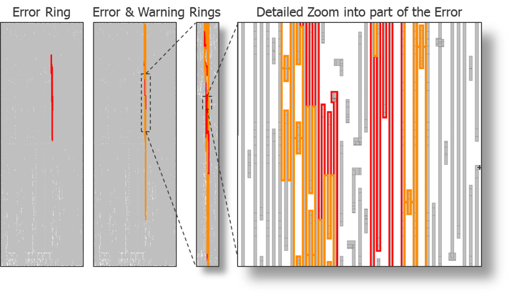
In modern P&R designs, the metal routes on a particular layer are unidirectional (or at least primarily unidirectional). Long pieces of metal are tightly packed next to each other across the whole block. Because of this general nature of automated routing, when odd cycle errors occur they can be very long. Large cycles can stretch across large portions of the block. When you turn on those very useful warning rings we discussed last time that help you debug the odd cycles, this display can seem overwhelming at first glance due to the skinny, long-range nature of the error that needs to be analyzed. Figure 1 shows what the error display can look like.
Figure 1. Odd cycle error and warning rings in P&R design block.
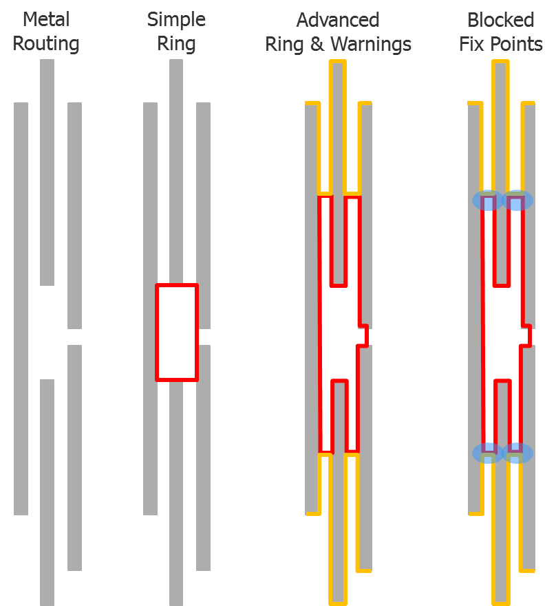
Because the error is so long and skinny, it is difficult to view without zooming into small regions, then panning up and down the error ring to see it all. In addition, the error seems very complicated because of the way the ring traces down between each pair of lines to the center point of their spacing interaction. Figure 2 helps explain this aspect of the display more clearly.
Figure 2. P&R odd cycle with simple and advanced ring visualization.
In this example, the metal routing has an odd cycle. If viewed as a simple error ring with no information about neighboring even cycles that can lead to new errors, you see the fairly simple-looking ring in the middle. When viewed with the extended visualization that includes the warning rings, the error rings are extended to the midpoint of each spacing interaction so you can see where they interact with an adjacent even cycle (partially displayed). It visually looks more complex, but it is the same ring with the same spacing interactions. You can now see that most of the potential spaces are blocked for fixes.
My first advice for designers is not to freak out about how large and complicated the error looks! You still evaluate it just like any other odd cycle. Use the display to zoom in to a point where you can see a reasonable amount of detail, and then pan around the error space, looking at all the error and warning ring interactions to see where a fix is possible.
Speaking of fixing these sorts of things, the nature of P&R layout leads to some interesting situations that are important to work through before you are in the middle of a tape-out, trying to figure out what you can do to get your errors resolved. Most of the time, we advise designers to focus on the spaces in the odd cycles, and look for one not blocked by a warning ring as a good fix opportunity. In a P&R layout, it is impossible to change the spacing between adjacent tracks. What you hope to find instead is a tip-to-tip spacing interaction in the ring, like the one on the far right of Figure 2.
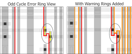
It would be simple to expand the gap between these two polygons on the same track, right? The problem is that tip-to-tip min-space interactions are notorious for causing odd-cycle errors, so most routers are configured to always use a larger space tip-to-tip on the same track to avoid this possibility. What does that mean? In my experience with real layouts, you never find a simple, same-track tip-to-tip space in an odd cycle to fix. What you are likely to find is something like the example shown in Figure 3.
Figure 3. Next-track neighbor short overlap configuration.
There are often locations along an odd-cycle error where two adjacent tracks have a min-space interaction, but the concurrent run-length of this space interaction is very small, as shown here. These interaction points can be great candidates for fixing odd cycles, as it is often relatively easy to pull the two lines back away from each other (as indicated by the yellow arrows) until the spacing interaction is broken and the odd-cycle is fixed. In this particular example, however, the warning rings prove their value, by showing you that this spacing interaction is also part of an adjacent even cycle. If you try to make this particular fix, it will only create a new, larger error.
In working with P&R designers on odd-cycle fixing, my experience shows that in the majority of cases, all of the spaces in odd-cycle errors are blocked by warning rings. This was initially very disconcerting, as it seems that there is no simple way to fix these issues. Some designers resort to inserting a routing block along an entire track involved in the cycle as a way to force the router to avoid creating it. This approach, however, can lead to less packing density, or failure to find a routing solution.
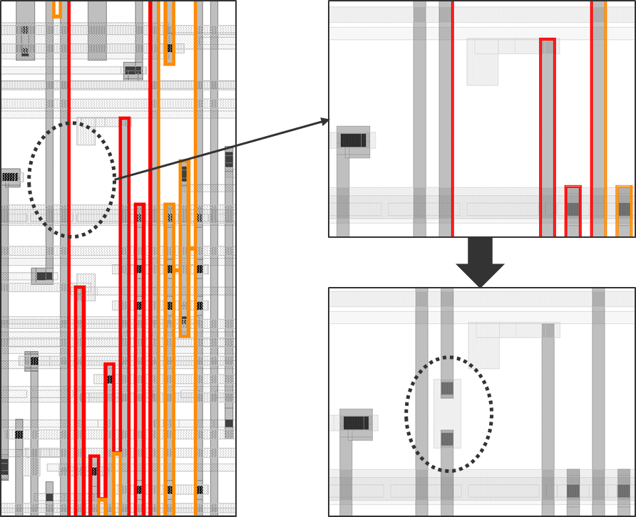
Instead, the key is to look at the problem differently and use the information coming from the warning rings in a new way. Instead of focusing on the spaces, focus on the lines themselves. As you scan around the error ring, notice where the ring runs along the side of a routing line, and then look to see if there is a warning ring on the other side of that line (Figure 4).
Figure 4. Odd-cycle fix using a jumper on lines that don’t have a warning ring.
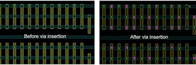
As you look at the left image, you can see that the entire right side of the odd cycle has warning rings running alongside it that block all the spaces and border most of the lines. These rings tell you that if you create a new gap in one of these lines in an attempt to change the alternation count in the cycle from odd to even, it would not fix the error. Instead, you would get a new error incorporating the neighboring even cycle. However, on the left side of the image, you can see that the leftmost routing line involved in the error ring does not have a warning ring running along the other side of it. This means you can insert a new break in this line to fix the odd cycle. The images on the right show an example of a “jumper” inserted in the routing to fix the odd cycle. It turns out that this technique is very effective in fixing odd-cycle errors in P&R design. It also shows how important the warning rings are to finding locations in which this technique will work.
One last issue I want to look at in P&R or chip finishing is actually a problem instigated by the cell libraries being used. With that said, it could be claimed that this is really a cell design issue, and not a P&R or chip finishing issue. However, in my experience with customers, the issue is never caught at the cell design level, and always ends up as a chip tape-out issue way down the line, when fixes are expensive and time-consuming. My hopes are that by pointing it out here, you can work with your cell library providers to ensure you don’t run into this issue when you are rushing to meet a tight tape-out schedule.
The issue has to do with density balancing. Most foundries have strict rules for ensuring a fairly even distribution of each mask color across the layout. They usually have density checks in the process design kit (PDK) to check the ratio of the colors in windows stepped across the design. Most shapes on a given design layer are similar in size, and since they tend to alternate in color due to their spacing to each other, they end up pretty well balanced in area per color.
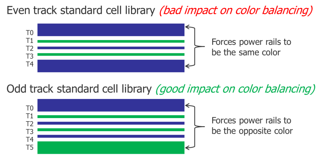
However, in a standard cell, the power and ground rails are usually much larger in area than all the other interconnect on a given metal layer. It turns out that the cell design methodology used can lead to or avoid density problems. Figure 5 shows the impact of two different cell design methodologies.
Figure 5. Comparison of the density balance between colors on different cell design methodologies.
If the standard cells use an even track library, as shown in the first case, the DP color alternation through the cell forces the power and ground rails to be the same color. They can be either blue or green, but they must both be the same color. Because these rails are large area polygons compared to the routing tracks, you get a significant bias towards one color. If, instead, the cells use an odd track library, then the power and ground rails are forced to be opposite colors. In this case, you get a much more evenly balanced coloring by area. Figure 6 shows how this manifests itself at chip level.
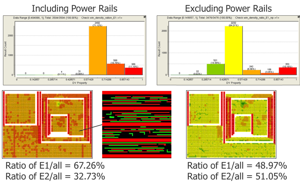
Figure 6. Even track library causing color density imbalance at full chip.
This chip used an even track cell library. When the chip was assembled and run through P&R, there were density-balancing violations all over the standard cell regions. The ratio between colors was 67% to 32%, specifically due to the power rails being forced to the same color. When we ignore the power rails, as shown at right, the rest of the polygons average an almost-perfect 50/50 ratio. This imbalance became a significant problem for the chip finishing engineer, as it required making changes in the library to try and get around the problem. This late in the design flow, making changes in the cells is very costly. The lesson to be learned? Make sure you work these types of issues out long before the chip comes to you for final assembly and tape-out.
I hope that these case studies will help P&R and chip finishing engineers understand and properly deal with some of the unique and interesting situations that can occur in DP processes. Knowledge is a key component of successful preparation. Take time upfront to educate yourself as much as possible on these topics, and contact your Calibre AE to help you out if you get stuck. A little self-education and preparation goes a long way when you’re fighting a tape-out deadline.
For engineers who are brand-new to multi-patterning, or who want to understand the basics of this technology, my white paper, “Introduction to Multi-Patterning,” gives you an overview of why multi-patterning is needed and a brief introduction to the different techniques now being used.
Author
David Abercrombie is the advanced physical verification methodology program manager at Mentor Graphics
Liked this article? Then try this-
Blog: Case Studies in Double-Patterning Debug, Part One
This article was originally published on www.semiengineering.com

