Will EUV Kill Multi-Patterning?
By David Abercrombie, Mentor Graphics
Many people think EUV lithography means the end of multi-patterning. Do you?
When I first began working on double-patterning (DP) tools back in late 2010, there was already talk that it might be a fruitless, or at a minimum, very short-lived project, as extreme ultraviolet (EUV) lithography was just around the corner and would make all multi-patterning (MP) obsolete. Well, as I begin my seventh year on this project, I can hear echoes of Mark Twain as clearly, the reports of the death of MP are greatly exaggerated! In fact, the opposite seems to have happened, with more and more multi-patterning processes being developed.
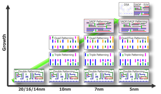
Figure 1 shows the almost explosive growth in MP techniques being examined, developed, and deployed in the foundries as we have pushed the technology nodes from 20nm to 7nm, and look forward to 5nm. Even now, it is still not clear that EUV will be ready in time for 5nm tape-outs.
Figure 1: Growth of multi-patterning techniques by technology node
At 20nm, the prevailing thought was that the cost and complexity of doing double-patterning would so severely limit the number of design companies that could afford to move to that node that it would be difficult for foundries to recoup the investment in fab capacity. Granted, there was a slower adoption rate of 20nm vs. previous nodes, but over time, a pretty large wave of customers moved into multi-patterned nodes. The advent of FinFETs at 16/14nm appears to have been a significant motivator. I have even seen some companies that were traditionally several nodes behind the leading-edge process users suddenly decide to jump into these nodes, leapfrogging over several nodes in between.
Now, as 7nm begins to go into production, some of those same notions of the cost of complexity challenges are being voiced again. In a recent interview, Craig Child, the Senior Manager and Deputy Director for GlobalFoundries’ Advanced Technology Development Integration Unit, made the following comment.
“For 7nm, the integration schemes are incredibly complicated. The mask count is going through the roof. If you look at just the back end of the line, the mask count is equal to what not very long ago was the mask count for the whole process. And the cost is going through the roof.”[1]
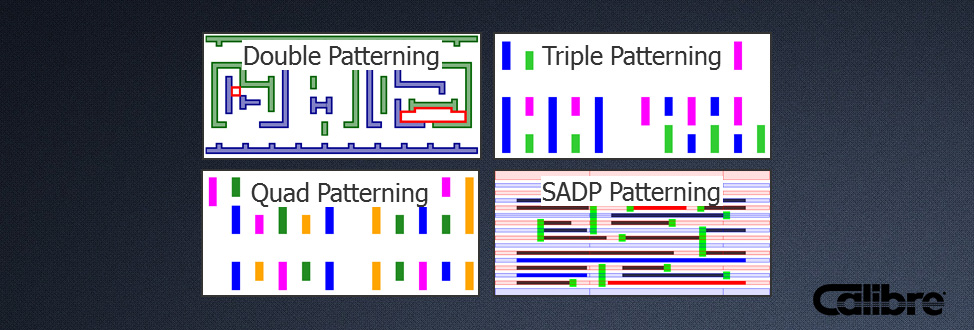
It is true that 7nm has become much more costly and complex because of the need to use not only DP, but also triple patterning (TP), quadruple patterning (QP), and self-aligned double patterning (SADP) multi-patterning techniques. There are many more masks in a 7nm process than there were in a 16/14nm process. This fact not only fuels the fears that few customers may adopt this node, but also fuels the call to convert to EUV lithography. The fact is, however, that with the current state of EUV lithography capability, these advanced multi-patterning techniques are still more cost-effective than using EUV.
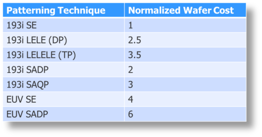
Figure 2 shows a comparison of normalized wafer cost for various patterning techniques, as estimated by Tokyo Electron Ltd. (TEL ). Clearly, multi-patterned 193i processes cost significantly more than single-patterned 193i processes, but as of today, a single-patterned EUV process is more expensive than any of the other techniques.
Figure 2: Normalized wafer cost adder for different patterning schemes [2]
You may have noticed that they included a multi-patterned version of EUV in the comparison. Why? Due to the continued delay in production deployment of EUV lithography, the tightest pitch layers on the leading edge technology nodes may not be printable with single-patterned EUV.
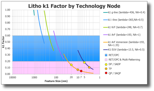
Figure 3 displays the trend of the lithographic k1 factor by process node and various lithographic systems. The k1 factor comes from a commonly used equation to relate the minimum attainable critical dimension (CD) of a lithography process given the wavelength of light (λ) and numerical aperture (NA) of the stepper.
K1 is a coefficient that encapsulates process-related factors. For the purposes of this chart, however, the λ and NA are fixed per the lithography tool being compared, and the CD is fixed per the x-axis. So if we solve for k1, we get the y-axis values shown.
Figure 3: Trend of lithographic k1 factor by technology node
As you can see, when you attempt to image a smaller CD using the same lithographic system the k1 factor falls. As this factor falls, there is less process margin in printing that CD. In fact, as k1 falls below ~0.6, the layout becomes non-yielding. But wait a minute! Given that fact, shouldn’t we have been out of luck manufacturing any node below ~500nm? Fortunately, more advanced lithography systems with improved λ and NA capabilities were developed, which helped the industry keep going. However, even with the most advanced i193 systems, we are well below 0.6 k1 on modern technology nodes. So how can we be manufacturing these nodes today?
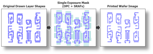
The answer is electronic design automation (EDA) software that incorporates optical proximity correction (OPC) and reticle enhancement techniques (RET), such as adding sub-resolution assist features (SRAFs) to the mask. With these functionalities, EDA software can modify the shapes that designers draw for their layouts in such a way that it counteracts the blurring inherent in the i193 lithography process. Figure 4 shows how this is done. The shapes put on the mask are significantly different than the shapes originally drawn. The end results, however, are printed images on the wafer that significantly match the drawn shapes to get yielding circuits, despite the lithographic system’s inability to directly print the shapes as originally drawn.
Figure 4: OPC Correction of drawn shapes to get yielding printed images on the wafer
Problems with the RET/OPC approach reached a head with the 20nm process, when we saw the k1 factor drop below ~0.2. At this point, the OPC modifications required for one individual shape overlapped with the OPC modifications of the neighboring shape, limiting the amount of OPC correction that could be applied to a design. This limited OPC correction was insufficient to result in good yield.
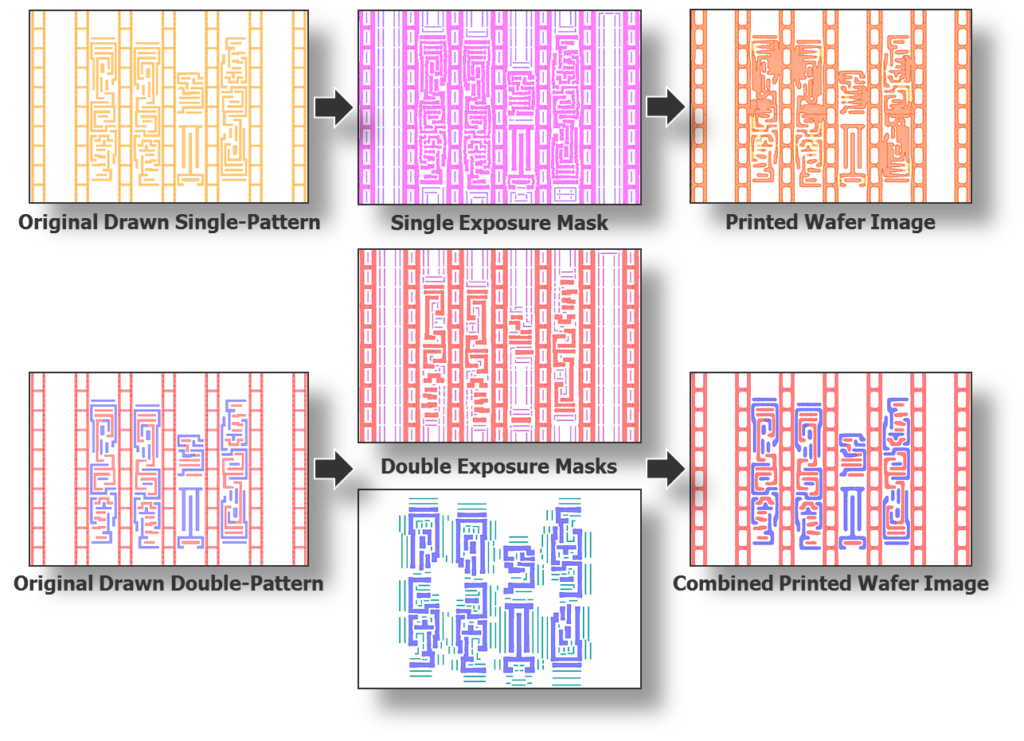
The solution was to divide the shapes between two separate masks, as shown in Figure 5. If all the shapes are on a single-pattern layer, then the OPC corrected mask is not able to produce good printed wafer images. However, if you split the original drawn shapes into two sets (commonly called colors), create a separate mask for each set, and print each mask separately on the wafer, the final result is a full set of yielding shapes on the wafer. The split leaves enough room around a given shape on a given mask to do sufficient OPC correction and get a good yielding print image on the wafer.
Figure 5: OPC Correction of drawn shapes to get yielding printed images on the wafer
The process of determining which shapes should be on which mask was automated through new EDA software with MP decomposition functionality. Again, just like with OPC, EDA software enabled what lithography is not currently able to do.
But once we get EUV, won’t all of this be a moot point? Well, looking back at Figure 3, you see the k1 curve shifts upward due to the improved λ and NA of EUV. If EUV had been available in time for 20/16/14/10nm, or even 7nm processing, then maybe MP would not have been needed. But it wasn’t. Now estimates are that EUV may be ready for 5nm. If you look at the curve in Figure 3, you’ll see that at 5nm, even with EUV, the k1 may fall below 0.2. If so, we will need MP to make EUV work.
Here’s another quote from the interview with Craig Child:
“EUV is not ready yet. It’s getting there. But the question we all need to ask is, ‘When is it going to be ready?’ Right now, we can do cuts and holes. We have processes that are capable. Can we do metal patterning directly? Not really. We’re not quite there yet. So you have this timeline for getting to this point, and the problem is when we get to the next node, is EUV ready? And if it is, do we still have to resort to multiple patterning with EUV. The assumption right now is that we get to the point where we can do one metal patterning and replace all of the metal patterning that we do now—the SADP, SAQP or whatever—with cuts. You take two or three masks out of the equation right away. But what if we’re at the point where the pitch has to go back to SADP. Then the cost benefit goes away. So we can see an EUV benefit, but it’s not clear if we can actually realize it.”[3]
Is he really suggesting that even if EUV becomes available, it may not provide sufficient benefit to make it worthwhile? That seems absurd. Maybe it won’t be able to print what we need with a single pattern, but surely a double-patterned EUV process would be much cheaper than a triple- or quadrupled-patterned i193 process, wouldn’t it?
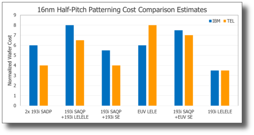
Figure 6 shows IBM and TEL estimates of the cost of various potential options for printing a 16nm half-pitch layer. Some use i193 solely, some use EUV solely, and some use a combination of both. The surprising thing about the comparison is that the solutions containing EUV are not the lowest potential options, but in fact, are among the most expensive ones.
Figure 6: Trend of lithographic k1 factor by technology feature size [4]
Now, don’t get me wrong. I’m not saying that we will never adopt EUV. But I am saying that even with EUV in play, i193 MP may still be the most cost effective option for some layers in some processes. In addition, the most advanced layers will probably require MP EUV. In both cases, it looks as though we should probably hold off on that obituary!
References
[1] Ed Sperling. ”BEOL Issues At 10nm And 7nm Experts at the table, part 1,” Semiconductor Engineering, Manufacturing, Design and Test. December 15th, 2016.
[2] Adapted from A. Raley et al. “A spacer-on-spacer scheme for self-aligned multiple patterning and integration,” Proc. SPIE 9782, 97820F (2016). https://www.researchgate.net/publication/306088534_A_spacer-on-spacer_scheme_for_self-aligned_multiple_patterning_and_integration
[3] Ed Sperling. “BEOL Issues At 10nm And 7nm Experts at the table, part 2,” Semiconductor Engineering, Manufacturing, Design and Test. January 4th, 2017.
[4] “16 nm hp Patterning Cost Comparison,” Wikimedia Commons, 28 September 2016. IBM: L. Liebmann, A. Chu and P. Gutwin, Proc. SPIE 9427, 942702 (2015). TEL: A. Raley et al., Proc. SPIE 9782, 97820F (2016). Guiding light at English Wikipedia [GFDL (http://www.gnu.org/copyleft/fdl.html) or CC BY-SA 4.0 (http://creativecommons.org/licenses/by-sa/4.0)], via Wikimedia Commons
https://commons.wikimedia.org/wiki/File:16_nm_hp_Patterning_Cost_Comparison.png
Author
David Abercrombie is the advanced physical verification methodology program manager at Mentor Graphics. For the last few years, he has been driving development of EDA tools that can solve the issues in design to process interactions (DFM) that create ever-increasing yield problems.
Liked this article? Then try this-
Blog: How Do I ECO a Multi-Patterned Design?
This article was originally published on www.semiengineering.com
