Here’s a set of candidates everyone can support!
By Wael ElManhawy – Mentor, A Siemens Business
Do you debug sub-20nm layouts? Want to make your life easier? Adopt an enhanced model-based hinting solution and maybe you can take weekends off, for a change.
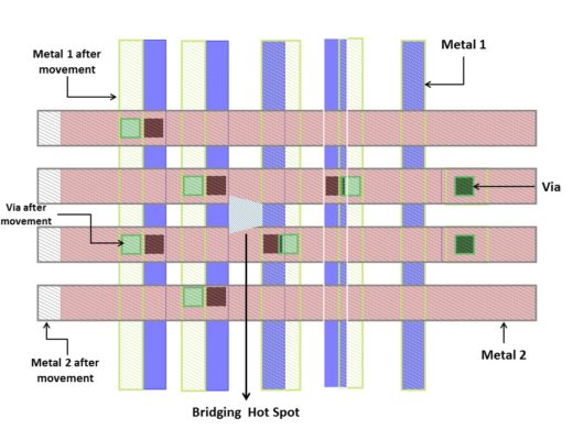
Traditional model-based hinting for lithographic hotspot fixing depends on individual local optimizations, like moving a single corner, a single line end, or the hotspot’s adjacent edges. But occasionally, these types of optimizations are restricted because of the strict design rules that apply to congested designs, like those found at 20 nm and below.
Here’s the good news—enhanced model-based hinting uses algorithms to identify a set of wire spreading candidates around the hotspot, in the event that the single local optimization can’t be performed. These algorithms can move entire polygons and multiple layers, instead of just single or dual edges.
I can hear you now, “Doesn’t that affect circuit connectivity? What about my DP coloring assignments? How do I know the design is still DRC-clean?” Not to worry—as the user, you can define a set of rules that ensure circuit connectivity, DRC compliance, and legal DP coloring are all maintained. The algorithm uses these rules as it evaluates the possible candidates, and whittles your choices down to the options that eliminate the hotspot without violating any of these constraints.
If you’d like to read more about the details, and see a few examples, download a copy of our white paper, Enhanced model-based hinting fixes multi-layer lithographic hotspots. If enhanced model-based hinting sounds like something you’d like to add to your verification toolbox, contact a Calibre representative for more information.


