Thrive and survive with Calibre in the Cloud
We recently participated in a presentation discussing something that is certainly creating a significant impact these days… Read more about a cloud-ready solution available to the semiconductor industry, and then watch the video.
Over hundreds, and even thousands of years, agrarian cultures around the world all developed rituals for invoking rain when it was needed to survive and thrive. From those rainmaking ceremonies evolved the modern-day business notion of the rainmaker, someone who brings large amounts of new business and/or money into their companies when no one else can. Now the semiconductor industry has its own rainmaker—cloud computing. Integrated circuit (IC) design and verification using cloud computing is creating a significant impact in the market, enabling companies to bring higher-quality designs to market faster, while remaining cost-conscious.
It’s no secret that IC designs are getting larger and more complex, while the technology nodes used to create them are shrinking down to once-unfathomable sizes. Companies are having a tough time getting these chips taped out on schedule, primarily due to the immense hardware requirements needed to run design rule checking (DRC) near the end of the design cycle. Most companies are forced to settle for long runtimes because they simply don’t have the compute power or number of CPUs needed for faster DRC fixing and signoff. Buying the resources you need really doesn’t help, because not only do you need a substantial capital budget to afford them, but you also must account for the time needed to acquire, install, and tune those resources. And even if you accomplish those acquisitions, you’ll be left with a significant number of resources that sit idle and unproductive for periods of time.
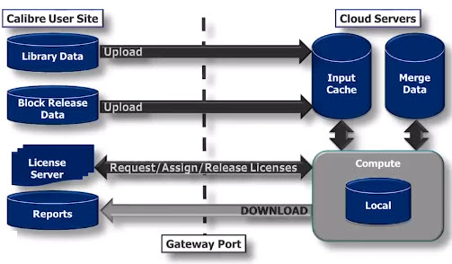
Combining EDA with cloud computing now offers companies another option. At this year’s TSMC OIP event, Mentor, a Siemens business, TSMC, Microsoft Azure, and AMD combined to introduce and explain their cloud-ready solution, which is now available to the semiconductor industry. Each company contributed their expertise to optimize their components and create a synergistic whole.
Mentor has always focused on improving the performance of the Calibre verification toolsuite node over node. However, to optimize their software for cloud computing, they took a closer look at specific strategies they could adopt, such as further optimization of memory usage, and changing the way the Calibre nmDRC tool acquired resources for hierarchical database construction. They also evaluated operational options to determine best practices, like using the cloud that is geographically closest to your physical location, and loading chip designs in a piecemeal fashion, rather than uploading a full chip layout.
In parallel with these efforts, Mentor worked closely with TSMC to further refine and optimize the Calibre rule deck to ensure that checks were being run in the most efficient manner. Mentor was also officially certified as a member of the TSMC OIP Cloud Alliance, which include auditing cloud security guidelines and practices.
Microsoft Azure, the cloud services provider, spent a lot of time to ensure they clearly understood both the resource demand curve and the requirements of each step in the design & verification flow, to determine the best Azure fit and best practices for cloud utilization.
AMD, who provides the high-performance processors that power the Microsoft Azure cloud, worked with all three partners to make an appropriate recommendation for each step in the verification process. The goal was to ensure cost-efficient use of appropriate processing power as needed throughout the verification flow. For example, the AMD EPYC CPU platform is well-suited for running Calibre; it is architected for massive parallelism. It provides excellent performance for jobs that require a lot of data processing (so you can use the IO) and scales well with threads, like the Calibre toolsuite.
All four companies joined together to present the results of their collaboration at this year’s TSMC OIP Forum in Santa Clara. For the design used, which was a 5nm testchip with over 500M gates and a GDS size of 17GB, they were able to reduce DRC runtime from 24 hours to just under eight hours. You can view the presentation here to get the full details of the project and the results they achieved.
If you’d like more information about implementing the Calibre toolsuite on the cloud in your organization, contact us! You could be the rainmaker that ensures your company not only survives, but thrives in the competitive markets of today.


