Automated ESD protection verification for 2.5-3D ICs is now a reality

Got the mid-winter blahs? The post-New Year letdown? Looking for something to rev you up? How about an automated method for ensuring your 2.5-3D IC designs are properly protected from electrostatic discharge (ESD)? If that puts a spark in your eye, the January issue of the IEEE Transactions on Components, Packaging and Manufacturing Technology has just what you need.
Dina Medhat, a senior technologist for Siemens EDA and Ph.D candidate at Ain Shams University, teamed up with Mohamed Dessouky and DiaaEldin Khalil, also with Ain Shams, to publish the results of efforts to build an automated checker for 2.5-3D IC ESD verification. This programmable checker can automatically detect different ESD protection schemes, and verify the corresponding ESD routing constraints implemented in each die. Data merging then verifies the integration constraints and identifies any violations at the 2.5-3D IC design level.
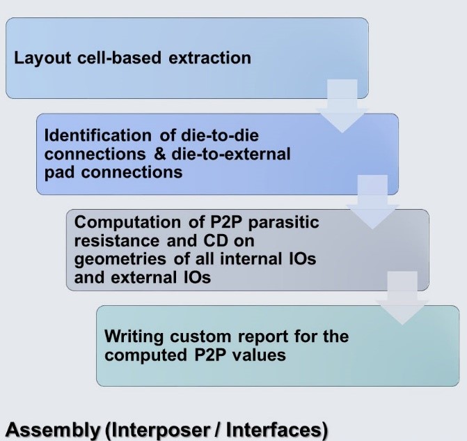
One of the key characteristics of the checker is its ability to differentiate between external and internal inputs/outputs from the assembly level without the use of manually-applied layout markers on the die level, which immediately reduces the chances for human error. It checks for correct, incorrect, and missing ESD protection circuitries for each category of inputs/outputs. It also checks total parasitic resistance and performs current density analysis for the relevant interconnect routes through the entire 3-D IC design layout to ensure these routes can sustain the ESD event.
They tested the checker against five dies: four random access memory (RAM) dies and a controller die. The checker accurately detected both missing/inaccurate and correct ESD protection, with the latter information enabling designers to also recognize “correct but unnecessary” protection that was using excessive chip area. For those correct ESD protection schemes, the checker also correctly verified total point-to-point (P2P) parasitic resistance and current density, and highlighted areas in the circuitry with the highest current density (indicating physical design issues that could benefit from remediation).
Their conclusions point to the value and practicality of an automated ESD verification solution for 2.5-3D IC designs to ensure accurate and consistent ESD protection. If you’d like all the details, you can read the full article here.


