Adaptive Patterning: Moving with the times (and technologies)

By John Ferguson and Kevin Rinebold
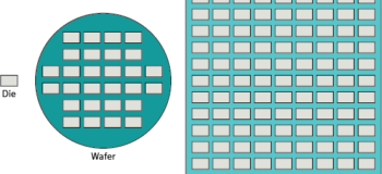
Deca Technologies’ Adaptive Patterning technology and their newly-announced adaptive patterning design kit (APDK) have the potential to revolutionize high-density advanced packaging (HDAP) manufacturing and make 3D IC more cost effective. How? By enabling panel-level manufacturing instead of using wafers. Okay…what does that do for us? Well, technologies such as fan-out wafer level packaging (FOWLP) are becoming popular because they enable significantly smaller physical footprint. However, in wafer-level manufacturing, a silicon wafer is used as a sacrificial carrier to create and hold the packaging stack in place, making this technique an expensive approach. Enter the panel…
While panels are a relatively new option in the industry, they are proving much more cost-effective than wafers. Die are attached to and the redistribution layer (RDL) is created directly on the panel. While the industry is still working toward a uniform standard size, panels are very big, at least compared to the size of a typical silicon wafer, meaning more systems can be assembled at once, and the mathematics of placing die on a square panel are much simpler, compared to a round wafer. Organic panels are also less expensive than a silicon wafer. As a result, the total cost per assembled package comes down significantly. Okay, you say, then what’s the catch?
The catch is that, for HDAP designs, you have to be able to meticulously place each die on the panel (so that everything lines up for connectivity) while still achieving the desired throughput. The process has to account for any placement/rotational skew of the die to enable routing alignment. In typical package manufacturing approaches, this translates into requiring larger bump sizes and pitch, limiting the overall connectivity.
And that brings us to why we’re talking about Deca’s new technology. Deca incorporates some pretty cool Calibre technology, in the form of our equation based checking (eqDRC) and programmable edge movement (PEM), as key components of the Deca APDK design methodology. They use Calibre eqDRC to measure exactly how far off the alignments are for each die placement vs. what was intended, then use Calibre PEM to dynamically adjust the routing of the RDL pattern on the panel so that the pins between die and package are properly aligned. These functionalities correct for the bump pitch limitations while taking advantage of the low cost and high throughput panel-based approach, enabling Deca to provide a fast, accurate, and highly-efficient panel-based process.
We’re proud to be a partner of Deca Technologies and, through the OSAT Alliance Program, to have been able to collaborate with both Deca Technologies and Advanced Semiconductor Engineering, Inc. in the development of this breakthrough technology for advanced packaging.


