So you think you know symmetry? Think again…

By Sherif Hany
“The Art of Analog Layout” is one of the canonical books addressing concepts behind layout design techniques used in crafting VLSI layouts. Although my professors insisted that layout is a science, and not an art, I’ve come to realize after years of working in design and physical verification that the word “art” simply reflects the size of the accumulated knowledge and the amount of manual intervention needed to craft a high-quality layout. It also turns out that this is not just true for analog, but for digital designs as well, especially for established nodes where the design requirements and complexity have exploded. Accumulated knowledge that is encapsulated in electronic design automation (EDA) tools can enable engineers to create high-quality layouts while minimizing the time spent in manual corrections and adjustments. This combination of knowledge and automation has a direct impact on design quality (performance), yield, and time-to-market schedules.
Although EDA suppliers and local CAD support teams try hard to introduce automation that will improve productivity, designers are often reluctant to adopt new techniques and tools, as they don’t want to add or change steps in their existing design flows that have been proven successful in several successful tape-outs, as complex as those flows may be. This is especially true for topics such as symmetry, which is typically thought of by designers as a mature design concept for which designers believe they have mastered all the techniques.
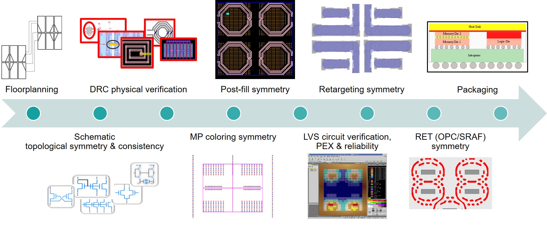
Actually, symmetry requirements have been evolving along with the growth in both design and process complexity. The design symmetry requirements derive in large part from new types of applications, such as Internet of things (IoT), automotive, and 5G communications that dictate more and tighter matching and reliability requirements, while new process technologies add extra steps that drive more symmetry requirements, from metal fill symmetry, device symmetry for chemical-mechanical polishing (CMP), and multi-patterning symmetry, all the way to optical process correction (OPC) symmetry and packaging symmetry.
At Siemens EDA, the Calibre team recently introduced innovative verification techniques that provide comprehensive matching and symmetry checking and debugging. While convincing skeptical designers to adopt the new technology was challenging, we’ve now seen multiple successful customer implementations across the whole design cycle. In fact, once deployed, the use of this advanced matching and symmetry technology quickly found its way beyond the intended applications to several new areas, such as quantum computing, silicon photonics, and MEMS, among others.
Maybe you’re a skeptic, too? If so, why not download a copy of our paper, Advanced symmetry checking in IC layout design and verification, and compare it to your current symmetry verification strategy and coverage? You might be surprised to learn how much performance and yield you could be missing out on.


