Do you need an automated ESD verification methodology for 2.5D/3D ICs? If so, read on…

By Dina Medhat
Electrostatic discharge (ESD) events cause severe damage to unprotected integrated circuits (ICs). You already know that, of course, because you’re required to add ESD protection schemes on both the schematic and layout, following ESD design rules included in design rule manuals. But now you’re faced with providing ESD protection for a 2.5D or 3D IC design. What do you do?
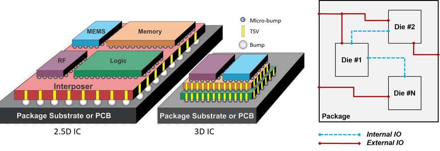
2.5D/3D ICs have evolved into an innovative solution for many design and integration challenges. 2.5D ICs have multiple dies placed side-by-side on a passive silicon interposer. The interposer is placed on a ball grid array (BGA) organic substrate, micro-bumps attach each die to the interposer, and flip-chip (C4) bumps attach the interposer to the BGA substrate. In 3D ICs, dies are mounted on top of each other, there are interfaces for communication between dies, and through-silicon vias (TSVs) are used for communication with the substrate.
So, can you just treat 2.5D/3D ICs as a group of independent 2D ICs connected together, and apply 2D IC ESD protection rules? The short answer is no. ESD devices can span multiple dies in 2.5/3D configurations, which must be combined for correct evaluation. Also, ESD events should be categorized for the different IO types. Internal IOs face fewer ESD events than external IOs. By identifying where these internal IOs are in the 2.5D/3D IC, ESD design engineers can place the appropriate smaller ESD protection circuits to avoid wasting chip area.
Implementing an automated ESD verification solution for 2.5/3D IC designs ensures correct and consistent ESD protection. At Siemens EDA, we formulated a systematic methodology to verify the ESD robustness of 2.5D and 3D ICs at three stages (assembly level, die level, and complete 2.5D/3D IC design level) that can be implemented using the Calibre PERC reliability platform.
Interested in the details? Download a copy of our technical paper, Automated ESD protection verification for 2.5D and 3D ICs.


