Balancing performance vs. debuggability in LVS circuit verification

By Wael ElManhawy
Circuit verification engineers face ever more challenges as semiconductor technology evolves towards smaller process nodes and integrated circuits (ICs) become more complex. Striking the delicate balance between speed and accuracy in circuit verification becomes paramount. This blog discusses the intricacies of managing this balance, particularly in the context of layout vs. schematic (LVS) verification and offers effective strategies for navigating these challenges.
The challenge at advanced nodes
At nodes of 10 nm and below, the landscape of IC design undergoes a dramatic shift. The area of standard cells shrinks significantly, leading to higher design density and increased complexity. With a surge in the number of transistors, metal layers, and connect statements, the need for rigorous physical verification becomes more pronounced. The increased design density and the presence of more complex device structures makes extracting an accurate netlist from the layout more challenging, with longer runtimes and higher resource requirements.
However, this need for thorough verification must be balanced against the imperative of meeting stringent time-to-market schedules, necessitating faster verification runtimes to adhere to tapeout deadlines.
I cover more of the challenges of advanced node LVS, including the problems with creating a manual hcell list for hierarchical debugging, in this technical paper “Managing the balance between performance optimization and debuggability in LVS circuit verification.”
The conundrum: performance vs. debuggability
The essence of the challenge lies in the clash between two crucial aspects of IC design: performance optimization (LVS runtime) and debuggability (quality of results). The initial phase of hierarchical LVS verification involves building an internal hierarchical database from the original input layout database. The Calibre Interactive interface features automated hierarchical hcell list generation.
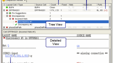
One main advantage of using hcells in LVS is that each hierarchical block is compared and errors reported with details about the possible cause of the violation, which can make the debugging process easier and more efficient. Figure 1 shows how these details are presented for debugging using the Calibre RVE results viewer.

The Siemens Calibre nmLVS tool uses techniques to optimize LVS run time, including automatically expanding certain cell placements to optimize the hierarchy. Using design hierarchy is a proven method to speed up LVS processing.
Runtime performance is generally better with a relatively brief list of hcells, which makes it easier to apply both design hierarchy modifications and optimize server performance. However, modification of the design hierarchy and expansion of layout cells can introduce problems for LVS debuggability because expanded cells will not be compared, meaning any errors between the schematic and layout will not be detected. On the other hand, using a large hcell list to ensure the best possible debuggability can severely impact runtime performance.
About Hcells
Hcells, or hierarchically corresponding cells, play a pivotal role in hierarchical LVS. These cells facilitate the comparison between layout and source netlists, enabling comprehensive error reporting with detailed insights into the possible causes of violations. By creating and maintaining a robust hcell list, engineers can streamline the debugging process and enhance overall efficiency.
While optimizing performance involves algorithmic modifications to the design hierarchy, expanding cell placements, and leveraging parallel processing, prioritizing debuggability requires preserving hcells to facilitate error detection and resolution.
A holistic approach to balancing runtime and debuggability
Finding the balance requires a holistic approach that fosters collaboration between circuit designers, layout engineers, and verification teams. By jointly defining the minimum set of hcells necessary for effective debugging while optimizing runtime performance, teams can navigate the tradeoff between performance and debuggability with finesse.
Smart selection of Hcell lists
The selection of hcell lists plays a crucial role in balancing performance and debuggability. By leveraging different options for hcells at various stages of the design flow, engineers can adapt to the evolving needs of the project. At different stages of the design flow, a Calibre nmLVS utility provides options for automatically generating different hcell lists that cover different ranges of hierarchy depths.
For more information on this, watch our recent video here HCELL flows update (siemens.com)
Coordination between designers and CAD engineers defines the level of hcells that are kept in these hcell lists. Using different options for hcells for different runs can offer designers more debuggability options by using a bigger hcell list in very early phases when designs are dirty, and help designers favor faster performance turnaround time by using a small set of hcells later on, when designs are cleaner.
The path towards managing LVS tradeoffs
In conclusion, achieving a robust and efficient circuit verification process means finding the right balance between performance optimization and debuggability. By embracing smart strategies for managing hcell lists, fostering collaboration across teams, and prioritizing the needs of the project at each stage, engineers can navigate the complexities of advanced nodes with confidence.


