Capacity Constraints and DFM at Mature Nodes
By Jeff Wilson, Mentor Graphics
Design for manufacturing – it’s a variety of practices that can improve yield and prevent defect.
We’re witnessing an interesting phenomenon in the SoC segment of the semiconductor industry today. One might call it the “forced waterfall effect.”
What I’m referring to is the tendency for production at semiconductor nodes older than the leading edge to be under long-term foundry capacity constraints. Normally this occurs with the “hot process node,” that is, the leading edge where the learning curve is still in a steep ramp. Yield is typically improving on a quarter-by-quarter basis, but it is less than what will eventually become the steady state output. This constrains the total number of available good die for a period, and if aggregate output falls below customer demand, foundries are forced to divide up what is available among its various customers—a process called “allocation.”
We may now be in a “perfect storm” where the usual leading-edge constraints are exacerbated by the hesitancy of many fabless semiconductor customers to move rapidly to the leading-edge node. This caution is the result of concerns about wafer cost, double patterning and finFET complexity, and design-dependent yield issues. Moreover, new Internet of Things (IoT) applications at the network end points are driving an uptick in demand for silicon based on established node process technology. The result is more-than-expected demand at 28nm and older nodes—hence the talk about allocation across all process nodes.
For many fabless customers, what a long-term capacity constrained market does is shift the perspective on design-dependent yield from…
“Should I invest more effort and time to get marginally better yield and reduce my costs?”
…to a different question:
“What can I do to get more net good die from my wafer allocation in order to meet my sales commitments?”
The good news is that for many fabless semiconductor companies there is a lot of “money left on the table” at virtually every node from 90nm forward, and there are effective design-for-manufacturing (DFM) practices that can improve yields. The fact is that many companies reluctantly have embraced DFM, and then only the absolute minimum that is mandated by foundries as a condition of signoff. Likewise foundries, being reluctant to have customers see them as difficult to do business with, have mandated only the DFM rules they absolutely need to avoid a yield disaster. The rest of the potentially advantageous rules are either designated as “recommended rules” or left off the sign off list completely. That’s where the hidden gold is for fabless customers who need to find ways to increase the number of good die available to them.
Design for manufacturing options
Design for manufacturing (DFM) refers to actions taken during the physical design stage of IC development to ensure that the design can be accurately manufactured. At larger nodes, many of the defects in the IC manufacturing process were due to out-of-tolerance process steps, i.e., a macro level variation, or random particles interrupting the flow of light through a layout mask during a lithography printing step or being embedded in a layer of the wafer itself. Process control feedback loops and better cleanroom procedures are effective in controlling these two mechanisms and have led to a reduction of random defects that impact wafer yield
However, as we moved from the 130nm node through 65nm, 40nm, 32nm, 28nm, 20nm and 16/14nm, the industry had expected that we would transition to EUV lithography to take advantage of shorter wavelengths for the lithography process. But due to delays in deploying EUV technology, the industry is still using light-based steppers with a wavelength of 193nm. As we learned in high school physics, diffraction effects become significant when the light interacts with objects and slits approaching the dimensions of the light wavelength. Obviously we have moved far beyond that threshold. At 130nm to 65nm, resolution enhancement technologies (RET), including optical proximity correction (OPC), also referred to as computational lithography, were able to deal with the general distortions caused by diffraction effects. This involves modeling the expected light distortions and making changes to the masks to correct for them so the resulting exposure on the wafer is correct as intended. Fortunately for IC designers, the RET step follows tapeout, so it has no impact on the design.
Unfortunately for IC designers, RET is not able to correct all the problems. As a result, IC foundries had to add design rules and DFM models that designers use to identify where design changes are needed to eliminate or modify features in the layout that cannot be accurately manufactured. At each node, the DFM rules become more complex, and the range of effects broaden in scope. For example, at 20nm, the rules governing fill shapes routinely placed in a layout to improve the consistence of metal across the die become far more complex, and the number of fill polygons increases by one or two orders of magnitude. Moreover, these defects are both systematic and contextual. Understanding how your specific design interacts with these potentially yield-limiting defects is how wafer yield can be optimized. The following sections have additional detail on specific DFM methodologies.
Litho hotspot analysis
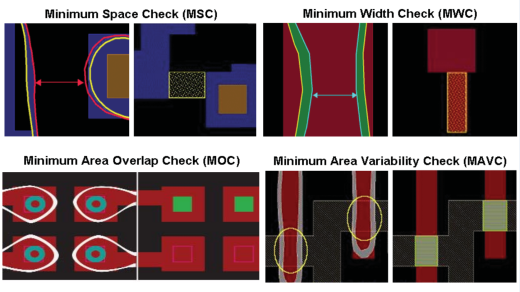
Figure 1. Lithography (litho) analysis involves simulating the effects of light diffusion and the impact of variations, like depth of focus and light intensity, on the rendition of intended shapes on the wafer.
Lithography (litho) analysis involves simulating the effects of light diffusion and the impact of variations, like depth of focus and light intensity, on the rendition of intended shapes on the wafer (Figure 1). A litho analysis tool gathers data about how the design will print over a range of conditions, such as variations in dose, focus, mask position and bias, not just at the optimal settings. These variations are referred to as the “process window.” The tool then predicts specific areas of the layout, i.e., shapes or configurations of shapes, that may result in a defect such as a pinched, broken or shorted interconnect wire. The impact of the process window is shown as bands on a graphical depiction of the manufactured layout. The bands show how the features will be rendered on the wafer at different values of the process window variables. Designers can review the hotspots and process variable bands and make improvement to the layout where needed.
CMP hotspot analysis
CMP hotspot analysis looks for areas of the design that have a higher than average probability of experiencing defects due to chemical-mechanical polishing (CMP). Because different materials will exhibit different erosion rates under the CMP process, it is important to maintain a density balance across the die to prevent bumps and dishing that can cause shorts and opens in the metal interconnects. CMP analysis measures various aspects of the layout to ensure even planarity as the chip is built up over multiple layers. Typical measurements include maximum and minimum metal (copper) density, density gradient over a defined window, density variation across the die, and the total perimeter of polygons within a window. A CMP model is used to analyze the layout and highlight potential hotspots before they happen.
It is important to note that the “fill” procedures normally performed at the end of the design process to add non-functional shapes in any empty (white space) areas of the design, were initially aimed at improving the uniformity of metal density across the die in order to help with CMP results. At advanced nodes the role of fill has become much more complex.
Advanced fill
In addition to improving planarity, fill is used to manage multiple manufacturing issues including electrochemical deposition (ECD), etch, lithography, stress effects, and rapid thermal annealing (RTA). This new role for metal fill in managing the impacts of manufacturing variation also includes managing the timing effects of added fill.
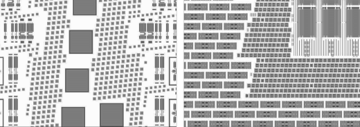
Each new process technology comes with many new design rules related to fill. For example, at 20nm fill shapes must be evenly distributed and also require a greater variety of fill shapes (Figure 2). Designers need to add fill not just to metal layers, but also to poly, diffusion, and via layers. In many cases, these layers are added together and referred to as multi-layer fill.
Figure 2. Fill has evolved extensively between the 65nm node (left) and the 28nm node, greatly increasing the number and complexity of fill shapes that must be added.
Another challenge for metal fill is controlling the turnaround time of the fill process. The time required for fill has been increasing due to both growing design sizes and the complexity of today’s filling process. At 20nm, the types and extent of fill analysis continue to increase. DRC density checks are still the standard, but they have moved beyond min and max densities. Density analysis is extended with gradient analysis (differences between adjacent windows). In addition, designers also need to achieve other constraints, such as perimeter and uniformity of fill spanning multiple layers. Meeting DRC constraints is a priority, but designers must also ensure that timing constraints are met. Advanced-node ICs require a balancing act between achieving density constraint and he amount of capacitance added to the design.
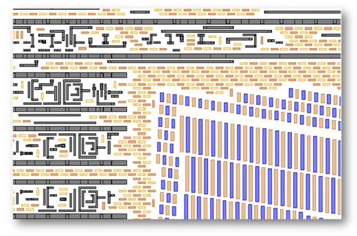
Finally, the addition of double patterning at 20nm adds a new dimension to fill (Figure 3). For drawn layers, double patterning improves printability. For fill layers, double patterning reduces manufacturing variability by balancing the light emitted through the mask and moderating the impact of etch on the design. Metal fill, like all the shapes in the layout, must be colored and decomposed into two masks.
Figure 3. At 20nm and beyond, fill must take multi-patterning into account, as shown by the different colored fill shapes in this layout.
As a result of this increasing complexity, designers can no longer use a simple “dummy fill” algorithm that uniformly fills in all white space with a single polygon shape at the end of the design. Because the latest designs can require billions of fill shapes, designers need to think about changers to their fill methodology. First, a “Fill as you Go” approach can help to minimize both the run time and timing impact of waiting until the end of the design process. Second, designers need a fill approach that can live within the constraints of an Engineering Change Order (ECO) process. ECO changes happen and will impact fill. The goal is to have a solution that only makes modification where explicitly required. Designers need a specialized DFM tool to address all these complex fill issues.
Critical area analysis
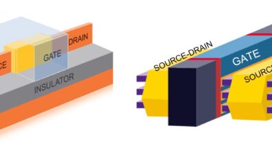
Critical area analysis (CAA) looks at an IC physical layout to determine if there are areas that might be susceptible to a higher-than-average rate of defects due to random particles. Defects typically occur when a particle causes a short or open in a chip interconnect. This is more likely to happen where the interconnect wires are either close together or minimum-width wires. CAA performs an analysis to identify so-called “critical areas” based on the spacing and dimensions of layout shapes, and the concentration and size distribution of particles in the cleanroom environment. Designers can then perform modifications, such as taking advantage of white space by spreading wires further apart in order to minimize these critical areas. With technologies that leverage finFET structures, new functionality also is required to account for the height of the defects.
Via enhancement
At smaller nodes, a significant number of defects result from poor via formation due to bubbles accumulated at via stress points, or due to a random particle at a via location. These issues can result in open connections or connections with excessive resistance. In addition, via transitions with insufficient overlap with the connecting wire also can contribute significantly to yield loss. A simple solution is to place two vias at each transition, yet doubling every via leads to other yield-related problems and has an impact on design size.
Special DFM tools can identify via transitions and make recommendations in the context of the specific layout as to where second via insertions are needed, and where they can be added without increasing area by taking advantage of white space. Such tools also can expand the overlap of metal over the vias to improve connectivity and reduce the potential for defects.
Pattern matching
As described under Critical Feature Analysis, some critical features cannot be described in a simple way—they are just too complex. To help designers find these complex features, physical verification and DFM tools now employ pattern-matching techniques. That is, a designer simply can copy a particular feature (portion of a layout) that has been identified as a problem and place it into a pattern library. The pattern matching functionality then can search an entire layout for all occurrences of patterns in the library. Of course, the tool must be intelligent enough to account for different orientations and placements of the pattern, and even small variations in dimensions of the pattern, as specified by the designer. Once the problem features are identified, designers can take appropriate action to modify or eliminate them. This topic is treated in greater detail in a separate Knowledge Center entry under Pattern Matching.
DFM scoring
DFM practices ultimately are focused on improving yield and preventing defects from showing up after a product has been delivered to a customer. Unfortunately, they also mean more work, which means more engineering costs—a classic engineering tradeoff. Designers need a way to tell when “enough is enough.” That is the purpose of DFM scoring, which is a methodology that uses a set of measurements of the physical layout to determine if the design is good enough to realize an acceptable yield. It looks for specific shapes and configurations that are known to be difficult to render on the wafer, and therefore have a higher probability of causing defects in the IC. These features typically are identified through simulation (as in the litho hotspot analysis described here), or though physical failure analysis on test chips or defective parts. Once the structures have been identified and correlated with yield loss, DFM Scoring presents the results to designers so that they can make an informed decision about the risk, and when they have put enough effort into DFM improvements.
Summary
DFM is not a single technique or tool—it’s really about addressing a variety of manufacturing issues during the design process. DFM practices ultimately are focused on improving yield and preventing defects that could present problems after a product has been delivered to a customer. These methodologies historically have tended to be foundry-driven because they are based on the design rules specified by the foundry, which are based on their experience and data from test chips and production chips at each node. However, designers need to make the final call on when they are done making DFM improvements. The goal is not just to deliver the required functionality, but to have enough parts to satisfy the market demand. DFM is an important function because it provides information to designers so that they can have an active role in delivering a design with the necessary yield.
Author
Jeff Wilson is a DFM product marketing manager in the Calibre organization at Mentor Graphics.
This article was originally published on www.semiengineering.com

