Case Studies in Double-Patterning Debug: Part One
By David Abercrombie, Mentor Graphics
Multi-patterning errors in P&R layouts can be intricate, and their solutions may not be obvious
Double patterning (DP) impacts just about every part of the design and manufacturing flows. However, the kinds of issues you encounter, the way they manifest themselves, and the ideal way to address them may be very different in different parts of these flows. I feel like I have spent a lot of time the last six months or so working with place and route (P&R) and chip finishing engineers on DP issues. I thought it might be worthwhile to share some of the case studies I have worked through with these engineers, and the real-world issues we faced and resolved.
All P&R product marketing staff are going to tell you beautiful stories of how their magical tool is DP-aware and will never cause a coloring problem. Think about it, though. All P&R tools have (supposedly) been DRC-aware for decades—when was the last time you streamed the output directly from a P&R tool to the foundry without running a sign-off design rule checking (DRC) tool like Calibre nmDRC on it? I’m guessing pretty much…never.
Now, I’m not suggesting that P&R tools are stupid or inadequate, but there are so many intricacies to putting a full chip together that a P&R tool has a hard time accounting for every single possible condition. We’ll see some examples of that in just a bit. Suffice it to say that every P&R and chip finishing engineer should be prepared to encounter DP-associated errors, and the challenges of determining what causes them and how best to fix them.
Let’s start with some apparently simple odd-cycle DP violations in a standard cell P&R design. Most P&R tools are supposed to be odd-cycle aware, right? So how could you possibly ever have an odd-cycle error in a P&R design? Well, it turns out that they are quite common, and they can be caused by some not-so-immediately-obvious sources.
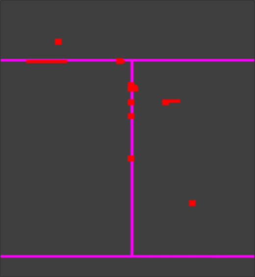
Let’s look at a couple of examples in Figure 1, which shows a portion of a standard cell P&R design. The purple lines represent the borders between several large, separately routed blocks. The red markers are various odd-cycle DP errors occurring in the design. You can see that many of the errors occur at the borders between the blocks, while a few occur in the middle of the blocks.
Figure 1. Odd-cycle DP errors in a standard cell P&R design.
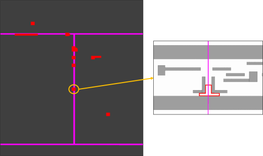
Figure 2 shows the detail of one of the errors at the block borders. When putting these blocks together, the chip-finishing engineer originally did not expect any errors, because the individual block designers claimed that the blocks were DP-clean after they finished P&R. When the chip-finishing engineer first started reviewing these errors, the purple layer marking the borders of the blocks was not highlighted, and it seemed that the odd-cycle DP error was occurring between two random adjacent standard cells. This initially led to lots of phone calls back to the block designers, because if the P&R tool was DP-aware, it should not have created these routing paths in this configuration. When they called me, I began by asking in which block, exactly, the odd-cycle was located. During that investigation, it became clear that the odd-cycle error was bridging across the border of two adjacent blocks.
Figure 2. Border spacing errors between blocks.
In the end, we determined that the issue was that, as each block was routed, the P&R tool was allowed to route within one-half the minimum space of the block border. Since the P&R tool had no foreknowledge of what was going to be placed next to that block, it happened to create these shapes at the block borders. Once the two blocks were abutted, they formed a minimum space error between the adjacent cells, forming the odd-cycle DP error. The fix required re-routing the individual blocks with a larger keep-out region around the block borders.
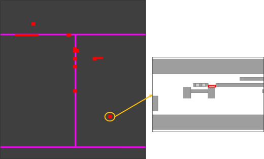
This condition explained many of the odd-cycle DP violations, but it is clear from Figure 1 that there are also some odd-cycle errors occurring far from the block borders (Figure 3). In this case, the error occurs right in the center of a single standard cell, and as such, cannot be explained by the first error condition. Again, if the P&R design teams were correct that the blocks were DP-clean after P&R, how could this error exist? In reviewing this error with the chip finishing engineer, we saw one thing that looked a little suspicious—the top left polygon in the odd-cycle error contained a redundant via configuration. It turns out that, in the chip finishing flow, a via-doubling utility was run using the P&R tool to improve the design for manufacturing (DFM) score of the design where possible. This utility was not DP odd-cycle-aware, so when it extended the polygon to the right to make room for the extra via, it created the DP error.
Figure 3. DP error caused by via-doubling script applied after P&R.
Frequently, I find that the biggest problem for P&R and chip finishing engineers is not just that DP errors occur, but that visualizing them can be very confusing when you are first learning to recognize and debug them. One thing that confuses and frustrates many engineers is that a single layout issue can potentially cause many different types of DP errors in the DRC run. Let’s look at an example in Figures 4 and 5.
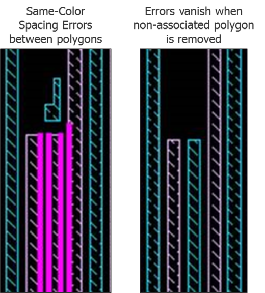
In this case study, the designer used Calibre nmDRC with Calibre Multi-Patterning to color a layout from a P&R design, and then run the DRC checks on the results. There were several DRC errors for adjacent polygons that were at minimum space with the same color. The left image in Figure 4 shows two examples of this rule violation, with pairs of pink edges marking the space between polygons of the same color. The initial, seemingly obvious, reaction from the engineer was to assume there must be some type of bug in Calibre Multi-Patterning. Why would it color adjacent polygons the same color if they are at minimum space? While waiting on a response from us as to what might be wrong with Calibre Multi-Patterning, the engineer decided to remove the small L-shaped polygon just above these two errors, just because it was a simple thing to do. To his surprise, the errors also disappeared, as shown in the image on the right. He also noticed that the color of the adjacent polygons now alternated properly. How could removing that non-associated polygon affect the coloring, especially when these two errors never even flagged that polygon?
Figure 4. DP same-color spacing violations mysteriously vanish when an uninvolved polygon is removed.
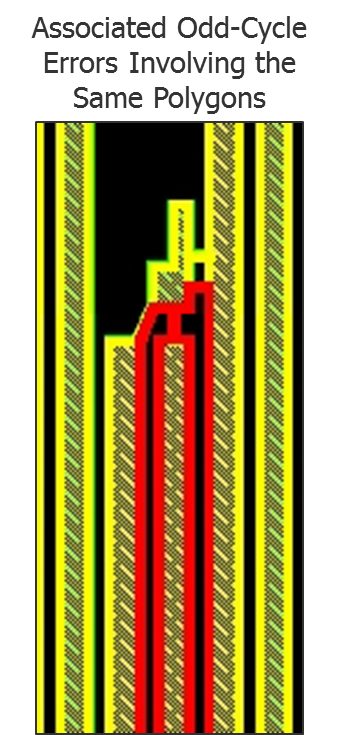
The answer to this conundrum was in a completely different DP rule violation. Figure 5 shows the error markers for the DP odd-cycle rule. You can see in red that there are two odd-cycle errors, both involving two of the three long vertical polygons that were originally colored the same color and the L-shaped polygon floating in the open space. But how does this relate to the same-color spacing violations?
Figure 5. The odd-cycle errors involving the same polygons kept the automated DP tool from properly coloring the polygons, creating the same-space coloring errors.
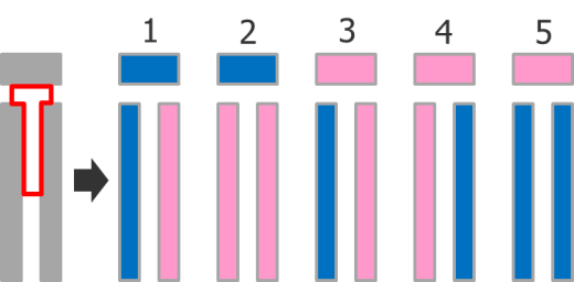
Figure 6 will help explain. The three gray polygons on the left form an odd-cycle error similar to the ones occurring in the P&R design. Because of the odd-cycle error, there is no legal coloring solution for the three polygons. Options 1, 3 and 4 cause a same-color spacing violation between the small polygon on the top and one of the long polygons. Options 2 and 5 cause a same-color spacing violation between the two long vertical polygons. Since all of the coloring options are equally wrong, the coloring tool randomly decides on one. Depending on which one it chooses, the original odd-cycle error then forces the same-color spacing violations to move to different locations. However, in our case, the designer inadvertently eliminated the odd-cycle error by removing the polygon altogether, which corrected both the odd cycle and same-color spacing errors.
Figure 6. None of the odd-cycle coloring alternatives provides a legal coloring solution.
While this can be confusing to a human, it is not an error in the tool. It simply reflects the fact that it is more efficient for a designer to review and fix some types of DRC violations before others (For more information on this topic, see my guide to DP debugging). In this case, reviewing odd-cycle errors first would reveal the root cause of the same-color errors, and fixing the odd-cycle errors would automatically fix the same-color spacing violations.
Another interesting case study involves confusion caused by something originally intended to reduce confusion, and it happens specifically in standard cell P&R designs. Let’s start by looking at the tool capability intended to reduce confusion. In DP layouts, it is common for one small odd-cycle error to actually obscure multiple overlapping odd-cycle errors (Figure 7). On the left, there is a small odd-cycle error involving the three polygons, highlighted with the traditional error ring marker. What is not obvious is that there is simultaneously an odd-cycle error involving all of the polygons. The layout modification shown on the right demonstrates what happens when the designer attempts to fix the original odd-cycle error by expanding the space between two of the polygons. Technically, this second odd-cycle error was always present, but trying to display both simultaneously causes confusion, because the larger one overlaps most of the smaller one. In these situations, a decision was made that it is generally better to keep the designer focused on the smallest source of the problem.
Figure 7. Fixing one odd-cycle error ring can reveal a second odd-cycle error.
However, because the designers do not know about the second odd-cycle error, their logical attempt to fix the first error will lead to the second error. In the Calibre Multi-Patterning tool, we developed a way to help designers avoid this situation without adding confusion to the original error (Figure 8). The Calibre Multi-Patterning capability can generate a warning ring (shown in orange). The warning ring tells the designer that the adjacent even-cycle interacts with the highlighted odd-cycle where they share the minimum spacing constraints between two polygons (i.e., the spacings that are spanned by both the red and orange ring). This warns the designer that if they attempt to fix the red odd-cycle error by fixing any space or moving any polygon that is also shared by an orange warning ring, the result will be a new odd-cycle error that now encompasses the polygons and spacings in the orange warning ring. This is exactly what happened in the first fix attempt above. By paying attention to warning rings, designers can attempt a different fix with a higher probability of success, such as the one demonstrated on the right.
Figure 8. Warning rings can help designers fix odd-cycle errors without creating or revealing new errors.
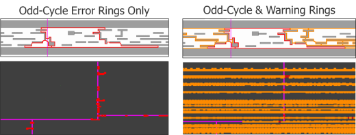
In general, warning rings give designers much more useful information with which to make intelligent fixes, but still keep them focused on the small error. However, in standard-cell design, a peculiar situation tends to happen that, upon first glance, causes shock to some engineers (Figure 9). Going back to our first layout, where there are some odd-cycle errors caused by large P&R block placement abutments, you can see on the left that several odd-cycle errors exist. In this case, the odd-cycle error spans between the power rails. Once the power rails are involved in an odd-cycle error, some interesting things can happen. On the right is the same layout with both the odd-cycle error rings and the warning rings displayed. You can imagine the initial shock when the whole standard-cell row lights up with warning rings. What exactly is going on here?
Figure 9. Comparison of odd-cycle errors with and without warning rings in standard-cell P&R design.
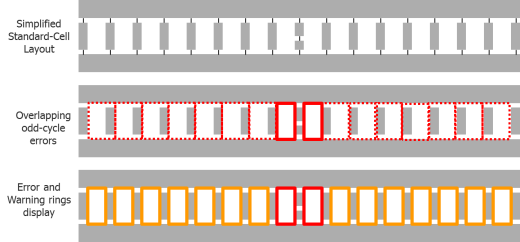
Let’s look at Figure 10 for an explanation. The top image shows a simplified example of standard cell design. The black lines show the minimum spaces that require color alternation. You can see that most of the standard cells in the row are configured such that there are two minimum spacing connections between the power and ground rail. This would force the power and ground rails to be the same color. In the very middle of the row is a cell that has three minimum spacing connections between the power and ground rails, which would require the power and ground to be opposite colors. This configuration is incompatible with the rest of the cells in the row, because it essentially forms overlapping odd-cycles across the whole standard-cell row (middle image). Showing all of these odd-cycle errors would be very bad, because the designer would not know which one was the root cause. To help the designer recognize this condition and make an accurate correction, the Calibre Multi-Patterning tool only shows the middle two standard cells (in solid lines) that actually isolate the root cause. The warning rings tell the designer that all those other cycles exist, and to avoid fixing the two red error rings by changing the outer sides, as that would just lead to another error.
Figure 10. Overlapping odd-cycles in standard-cell design.
Once you understand what is going on, the error display makes total sense, and actually ensures you stay focused on the very middle location where the two red cycles interact, instead of trying to fix them on their outside edges. However, the sheer volume of warning ring output can initially be quite disconcerting, as it looks like a huge problem exists when the whole row lights up. Educating the designers so they understood what was happening and what the output was telling them enabled them to work very efficiently at debugging and correcting these types of DP errors.
P&R and chip finishing engineers have some unique and interesting situations to deal with in DP processes. Take time upfront to educate yourself as much as possible on these types of DP errors. When confronted with a display full of red and orange rings, do not panic (and keep your towel handy). What may look strange or seem perplexing at first will most likely make complete sense once you calmly review all the error visualizations and think through exactly what is happening. You can always contact your Calibre AE to help you out as well. If they get stuck, I’m confident I can help them figure it out for you.
Next time, we’ll look at a few more case studies of DP issues that are specific to P&R and chip finishing, and discuss the solutions.
Author
David Abercrombie is the advanced physical verification methodology program manager at Mentor Graphics
Liked this article? Then try this:
Blog: Case Studies in P&R Double-Patterning Debug Part 2
This article was originally published on www.semiengineering.com

