Placement Challenges: Training is a Two Way Street
This is the third post in this series. View the first and second one.
In this series we have talked about the placement challenges that occur when we, as PCB designers, do not get complete information from the engineers. Without enough information, we can’t move forward independently.
So, how do we correct the issue? Training. But, in order to create a “rock star” design team, training must be a two way street.
First, the engineers must have confidence in you as a PCB designer. To build that confidence, they might need to work closely with you for a while as they train you in the method by which they like to see specific circuits and components placed. Engineers like to be very exact with their circuits, and two different ones may place the same circuit slightly different based on their application. As a PCB designer, you must take note during this training as your training of the engineer comes next.
As you start to gain the trust of your engineer, show them what you require as a layout designer for a high quality design that is completed in an efficient manner for a faster turnaround time.
We need to teach the engineers to provide complete information for their design, and not just notes and statistics – but true design layout intent from their perspective.
One method of providing intent is constraints, but often getting the engineer to add constraints to their schematic requires them to learn a complicated constraint system (and most will not even try).
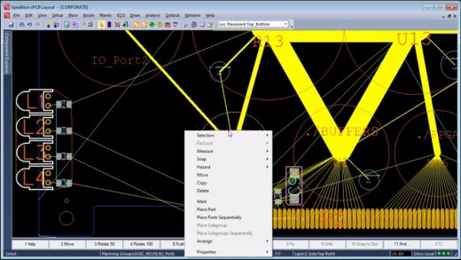
But, we want placement intent. As demonstrated in the previous posts, the engineer can now provide some of that intent directly from the schematic. This includes placement information such as circuit grouping and even circuit group locations or rooms. Groups can be passed to the PCB designer and layout directly, adjusted by the layout designer, and then passed back for review when needed. Then these groups can be used to rapidly floor plan a layout placement and easily reviewed prior to starting the finer and more intricate circuit placement.
Imagine that your engineer has created a FPGA design with a 2000+ pin device and hundreds of decoupling devices. What if the engineer grouped the decoupling devices hierarchically based on the functional banks of the FPGA? Would that provide intent? Of course it would, and it would be much better than a sheet in the schematic with thousands of decoupling devices to try and figure out.
What about re-use circuits or channels that are duplicated from the current or previous design? Pre-grouping these circuits will allow the layout tools to use copy circuit technology better to quickly place these groups.
With a bit of increased how-to knowledge, engineers can provide better information based on their intent, and it can easily be done right in their own schematics.
We will all make better design teams by sharing information in both directions. Take a look at this video on some other capabilities that can be passed from the schematic. But, if you have to do it old school, I have also provided a link to a design guidelines document [HERE] that I have used for many years. You are welcome to use it to help train your engineers. With the right information from your engineers, you are further empowered to design the best possible layout.
Comments
Leave a Reply
You must be logged in to post a comment.


Because this is so simple and easy to do I see passing placement intent as gaining wide acceptance once everyone is exposed to it. In my experience it’s been hard to get the circuit designer to accept that while drawing the circuit they need to think forward to how that schematic will be read and used in the layout process. Here’s hoping that Component explorer will better explain why it’s so important and provide tha means to do it.