Designing PCB’s for IoT – Part 2: IoT Design Domains
This is Part 2 in a blog series examining the unique aspects of IoT PCB design. Click here to read Part 1: IoT Everywhere.
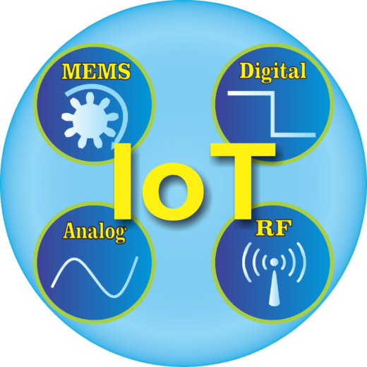
Fitness trackers monitor metrics such as distance walked or run, calorie consumption, perhaps heartbeat and sleep patterns. They sync wirelessly with smartwatches, computers and smartphones. Though they may look sleek and uncomplicated from the outside, even the smallest IoT devices can and do have some very complex, miniaturized and mixed circuitry including analog, digital, RF and MEMS that need to work together on the inside.

Fitbit Alta family
Analog-to-digital (ADC) converters are used in IoT designs to process, store, or transport virtually any analog signal in digital form to a microprocessor. The key advantage of analog is that is offers an infinite number of representations, while digital has a finite number of possible representations. Converting from the analog world to the digital world enables us to use electronics to interface to the analog world around us.

MEMS (Micro-Electro-Mechanical Systems) are the miniature sensors that gather information from their surroundings while actuators execute given commands. From fitness trackers that detect your steps, to a smartphone sensing when you’ve tilted your phone and rotated the screen, MEMS are key components in many IoT design.
Of course all of these IoT devices must also connect to the Cloud via WiFi, Bluetooth®, or custom protocols. This is where RF (radio frequency) comes in to play. Multiple factors including application needs, technology constraints, and different hardware and software integration requirements must be considered for wireless connectivity.
IoT devices, like any product, must fit a need or solve a problem for consumers and businesses. For consumer wearables like fitness trackers, they must also be user friendly and fashionable. Supporting the features and functionality of these small complex designs is a challenging task as designers must consider the unique domains of analog, digital, MEMS and RF throughout the design process.
Part 3 of this “Designing the PCB’s for IoT” blog series will look into the unique form-factors and components in IoT PCB designs. To learn more, download my white paper: 7 Design Aspects of IoT PCB Designs.
Thanks for reading!
John
Comments
Leave a Reply
You must be logged in to post a comment.


Very Informative. So much to pack in much less space, IMUs, MCUs, Radio, Anteenas(now a days on PCBs itself), OLED displays etc, definitely PCB design is a crucial part of such products, saving space and ensuring all design rules checks is a complex task. Keep Sharing.