Layout automation using advanced PCB design techniques – Part 1
Over my 25 plus years of being a PCB designer I could not imaging going back to designing a PCB like I did in the late 90’s or even early 2000’s. New technology is always being added to tools we use that helps simplify our job. The key is making sure you’re aware of these technologies in both the tool you’re currently using and others in the industry. If you’re not using advanced techniques like high-speed routing and tuning, placement planning groups, design reuse, plane generation automation and many more, it could be delaying your design completion time up to 70% or more. In some cases 90% when implementing auto-routing technology which we I’ll be discussing. You’re essentially giving your competition a competitive advantage. PADS Professional provides all of these advanced PCB design capabilities and more empowering small teams, independent designers and engineers to fast-forward product creation.
Placement
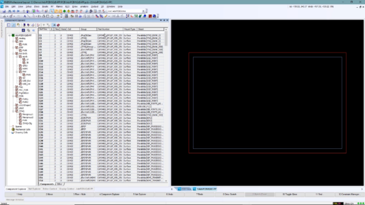
Most designers start a PCB design by grouping parts using cross-probing from the schematic. However, using a spreadsheet based view like Component Explorer in PADS Professional (Figure 1) allows us to quickly see information about our components and groups created for each circuit. These groups can be created either in the Schematic or PCB layout.
Today, every design contains some sort of IO interconnect, visual indicators, and mounting features that need to interact with a mechanical enclosure. In most cases, the mechanical engineer will define the locations of these objects and even place 3D models to support his/her design efforts. PADS Professional includes industry standard ECAD/MCAD collaboration allowing the ME and EE to exchange data using visualization and electronic data.
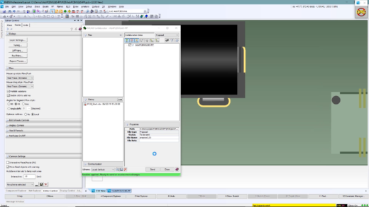
This design example is started by using collaboration data created from Siemens NX. Our ME created the board outline, mounting holes, and connectors based on their mechanical design. In less than a minute we’ve done the work that would normally take 60+ minutes (Figure 2). In addition, if using drawings, we would have a higher chance of making an error. Watch our archived webinar on MCAD collaboration to see more details.
Download a free trial of PADS Professional today!
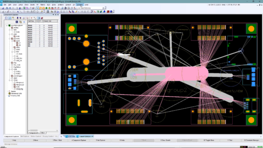
Creating a rough placement while seeing interconnect using groups allows us to plan our placement without placing a single part (Figure 3). While placing groups, net lines are visible which vary in thickness based on the connection count. The circle size for a group is defined by the component size and count. More importantly we can see net topology between groups which helps determine routing paths and where there may be congestion. In addition, we can create hierarchical groups, one large group for the entire circuit and sub-groups for items like termination resistor, decoupling, etc. This allows us to use additional automation for parts to be placed on the bottom or at a particular rotation which can be assigned to each group or sub-group.
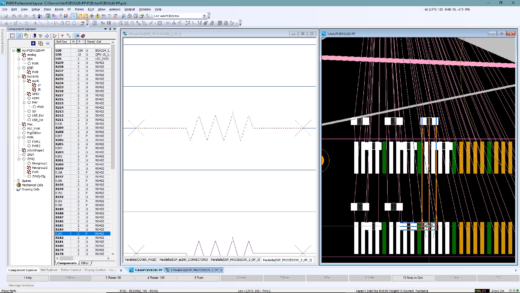
Most every schematic and PCB tool can cross-probe to assist with placement, PADS Professional can as well. However, to simplify this task we can use an embedded schematic viewer with simplified controls (Figure 4). Passive components always pose a challenge to place with the large number in a design. Finding passives via the schematic and using sequential placement makes it a snap. While placing the termination resistors for this connector we’ll use alignment technology to speed placement. As each part is placed and lines up with the axis of another, the part snaps to the edges of that placed component. Unlike component distribution in most tools, PADS Professional can auto-arrange parts for a group using their placement outline and design rules.
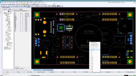
A 2nd method for placing parts from a group is to right-click over the reference designator of a group and choose from the list (Figure 5). This minimizes mouse movement facilitating faster design. At some point we always need to move a group of parts. Because we created groups for the majority of the parts in this design we can use the visible group outline to move a selection of components easily.
Design reuse
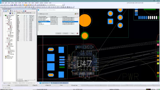
The ultimate in time saving technique is to use circuit reuse from one design to another. Design reuse can be done for both the schematic and PCB. Our design contains 2 USB interfaces that use the same circuit but different connector. The connectors were placed via MCAD collaboration, for the remaining components and routing we will use design reuse.
Layout reuse includes all items that can be created in a layout along with those selected upon creation (Figure 6). Which can include; part placement, traces, planes, vias, drawings, keepouts, stack-up, manufacturing data, etc. If reference designator values from the saved reuse and the current design are the same you have the option to automatically choose the correct parts. If there’s no reference designator match, you can auto-resolve part selection and interactively select the appropriate part for those that do not have a single match. Once placed, the circuit can be customized based on surrounding circuits.
Download a free trial of PADS Professional today!
Stay tuned for Part 2 of this blog series!
