ABCs of PCBs – O for ODB++
Welcome to ABCs of PCBs – a blog series to help new engineers learn about the world of Printed Circuit Boards. I’ll be covering topics from general engineering concepts to PCB design specific rules. As this is a ‘basics’ blog, I’ll keep the content software independent, but any visuals will be from the Mentor PADS Professional PCB suite.
If you missed the last post in this series: ABCs of PCBs – N for Netlist click here!
Previously, we discussed manufacturing tests you can run on your designs to make sure you’re sending the best designs for your manufacturer to produce. These tests are incredibly beneficial to the PCB design flow – but not the type of test results that are sent to a PCB manufacturer. You instead must output/export files generated from your design tool specifically for manufacturing.
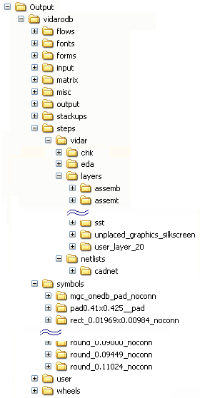
ODB++ (Open Database) is a standard data exchange file format that generates PCB design data files for use in fabrication, assembly, and test. Unlike other formats, ODB++ is structured in a hierarchy of files. This preserves and stores a larger amount of important data to be transferred between designers and manufacturers, like drill charts and placement. In fact, many PCB design tools have a built-in File > Export ODB++ file creation option.
When generated, this file can then easily be sent out to your manufacturer. Some of the files found in an ODB++ include drill data and BOMs:
Drill Data
Drill Charts are graphic charts (see above) generated by the PCB design tool and located on the PCB fabrication drawing. These charts specify all of the drill hole sizes, each with a unique symbol and include the hole sizes, tolerances, quantities, and whether the hole is plated or not. NC (numeric control) drill files contain comments to identify certain characteristics in addition to the types of holes that must be drilled, punched, or routed. This data is fed to manufacturers to make sure the proper drill category is used.
BOM
You can probably guess what information is stored in a bill of materials (BOM). It’s fairly self-explanatory – a BOM is a list of all parts and materials required to assemble your board. This file usually lists the quantity of each component and piece-part and often each item’s price. Some PCB design tools have the ability to link with part manufacturers like DigiKey and Mouser to provide you with accurate and up to date pricing and availability for the BOM. With tools like these, you can provide alternate sources of supply for components that ensure that the size and parametric data you’ve specified in the schematic and layout match the components you’ll be ordering for your finished product.
As you prepare your PCB for fabrication it’s important to check with your manufacturer to see which output files are required. While most accept ODB++ formats, some may be limited to a Gerber file format, so be sure you’re sending in the correct type of file. If you would like to learn more about the ODB++ file format, check out their website here.
To avoid confusion: Though the format is the same, the name “ODB++” is now synonymous with “ODB++Design”.
Are you a student? If so, try your hand at designing and testing a PCB with the free PADS Professional Student Edition.
Thanks for reading and see you next time for more on the ABCs of PCBs.
-Shivani Joshi


