FPGA/PCB co-design with PADS Professional Premium

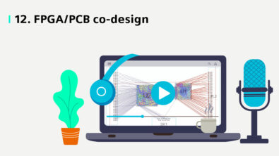
As the complexity of today’s designs continue to increase, more electronic product designers are turning to Field Programmable Gate Arrays (FPGAs) to bring more functionality to the PCB design. The benefits of using FPGAs include better performance, programmability, cost efficiency, faster time to market, and many more. However, the high pin count of these devices also brings challenges, such as difficult routability, longer trace lengths, more vias, an increased number of layers, and signal integrity issues. When using an FPGA in a design, bridging the gap between the FPGA and PCB domains is crucial for optimizing the FPGA IO within the context of the board.
Integrated I/O optimization
Having an I/O optimization capability that is tightly integrated with the PCB design flow, accessible at any stage of the project, is essential.
This starts with the definition of the FPGA device. By grouping pins across the FPGA’s I/O banks, the optimizer provides more flexibility in pin assignment. These groups can be treated as separate HDL entities within the tool and can be created manually or extracted from an HDL file (Verilog or VHDL). The advantages of pin partitioning include better PCB connection planning, customized symbol generation and minimizing the pin swap rules within the group, leading to better control of pin optimization and improved net unravelling.
A correct-by-construction FPGA vendor rule-driven I/O assignment minimizes re-spins, while a comprehensive library of FPGA vendor devices minimizes setup time and eliminates manual error.
Improved routing
An important phase of the PCB design flow is placement and orientation of components on the board. Using an integrated floor planner allows optimization of the FPGA I/O for improved routing. Since the I/O banks/groups have been defined, once components are placed, true IO optimization will “unravel” net lines by allowing pins within banks, that are defined as swappable, to change their pin assignment. This reduces layers, minimizes signal integrity issues, shortens traces, and reduces the number of vias used.
A comprehensive library of FPGA vendor devices
A comprehensive library of FPGA vendor devices minimizes setup time and eliminates manual error. Siemens provides support for the latest FPGA devices through partnerships with the leading FPGA vendors. It fully supports the following FPGA vendor tools:
- Altera Quartus II
- Lattice Diamond and ispLEVER
- Microsemi Libero and Designer
- Xilinx ISE and Vivado
For more information about FPGA-PCB Optimization, download our eBook.


