PCB design best practices: analog mixed-signal (AMS)

What is analog mixed-signal analysis?
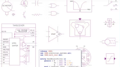
Analog mixed-signal circuit simulation (AMS) is a technique for analyzing circuits in an integrated environment for analog/mixed-signal behavior, supporting advanced modeling techniques based on SPICE and HDL.
This technology takes SPICE-based circuit analysis to the next level by leveraging the latest industry advancements in PCB modeling and simulation. It helps speed up circuit development, simplifies verification, and empowers designers to create boards that meet specific requirements. With a wide range of standard time and frequency domain analyses, along with comprehensive model libraries, you can thoroughly explore performance sensitivities, analyze statistical behavior and manufacturability, identify worst-case scenarios, and calculate component stresses using advanced design analyses. Plus, you can even build virtual prototypes of your board designs and subject them to rigorous testing, all while ensuring compatibility with the end system.
What’s not working today?
With today’s PCB designs being more complex than ever before, a legacy approach simply isn’t going to work. Manual analysis checks, limited tool capability, and or skipping the step of running a signal analysis/simulation to save a few bucks or a few days in the project budget, is proven to have a high potential for unnecessary respins.
Maintaining the legacy outdated ways of designing PCBs may mean that your company won’t be competitive in today’s market. An outdated mindset to meeting today’s challenging complex designs under tighter project schedules, resources, and budgets has the potential to be detrimental to a company’s long-term success.
What are the roadblocks?
Typical roadblocks that exist today that prevent engineering teams from implementing industry best practices are higher project demands, shrinking project budgets, and limited resources. Many companies have implemented a standard design process within their ecosystem, but most don’t have this process captured (written down) as part of their standard operations flow. Not having a standard design process in place leads to a non-optimized process, inefficiencies, and the potential of lacking domain/discipline expertise and or specialists working in silos. All this leads to a high potential for variations in the design process, skipped steps, and multidiscipline and multidomain integration issues. Ultimately, leading to repeated mistakes carried over from one project design to another causing un-necessary respins.
Another roadblock is internal company culture. In this roadblock, I am specifically addressing not having access to adequate design/analysis/simulation tools that are more than capable of meeting today’s challenging complex PCB design needs. This includes reduced/limited departmental engineering tool budgets to obtain such industry tools. Then, add in having those team members who are not open to adapt/evolve with industry best practices to meet tomorrow’s designs today. Sometimes, an internal company culture itself can be a company’s biggest hurdle to deal with when it comes to change/evolution.
Best practices: analog mixed-signal analysis
The best practice is to include analog mixed signal analysis within in your design process from the earliest electrical design stage and throughout final release of the PCB design. Don’t skip AMS simply to reduce project design time or engineering cost to meet project schedules. When skipped or neglected, there is a high probability that it will come back to haunt you!
Siemens has integrated Xpedition with HyperLynx advanced 3D electromagnetic solvers to incorporate board level parasitics in the circuit design process where it is most efficient to make design changes. Accounting for layout parasitics early in the design process reduces risk of downstream design iterations and is key to keeping a project on time, on bud¬get, and working to specification.
PCB parasitics can be a crucial factor in modern analog / mixed-signal designs, but their effects on circuit behavior are usually ignored during design simulations. This can result in designs that miss their performance targets or must be manually tuned after manufacturing. Integration between Xpedition AMS and HyperLynx Advanced 3D EM Solvers allows PCB parasitics to be accurately modeled and included in AMS simulations before PCB fabout, so that design adjustments can be made quickly and accurately, greatly increasing chances of first-pass design success.
How it works: analog mixed-signal analysis
Detecting potential signal quality issues at the early stages of the design process is crucial for reducing the need for design respins. Xpedition Analog Mixed-Signal circuit simulation (AMS) takes standard SPICE-based circuit analysis to the next level by incorporating advancements in PCB modeling and simulation. This not only expedites circuit development but also accelerates the verification process. With the ability to drive everything from a single schematic, why go through the hassle of drawing circuits twice?
Xpedition analog mixed-signal seamlessly integrates with the Xpedition design flow, so the schematic you use for simulation also effortlessly transitions your design to layout. With advanced design simulation, we can go beyond standard time and frequency domain analysis to explore design sensitivities, sweep circuit parameters, determine manufacturing yields (including corner-case behavior), and analyze worst-case performance. You can verify design performance using a virtual prototype of the target system. Plus, we offer a wide range of device modeling choices, leveraging component vendors’ SPICE and PSPICE models. And let’s not forget about VHDL-AMS, the industry-standard language for modeling AMS and mixed-technology design behavior, which expands your modeling and analysis capabilities.
To learn more about analog mixed-signal analysis visit our website.


