Tailor Your Approach to PCB Layout
Why fumble around with a GUI that makes you search for settings and switches? Your time is valuable! With PADS Professional, you can create a highly intuitive, tailored approach to PCB design that is unique to the way you work. An advanced customized GUI, placement, and 3D are three of the core technologies in PADS Professional that will speed your design process. Let’s take a look inside.
Fewer clicks
First we’ll take a look at the GUI. Optimized for usability, speed, and user customization, a context-sensitive select mode drives tool operation, reducing the number of clicks in day-to-day usage. Just select an object and get context-sensitive menus and actions.
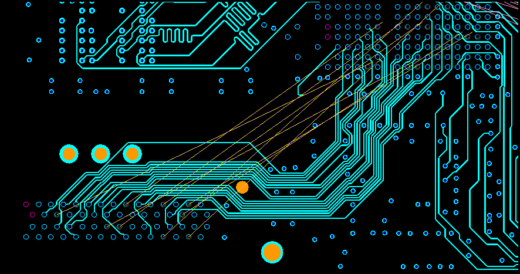
For example, interactive routing just requires one click on a pin to start the route. Routes autocomplete as you get near the target pads, meaning one click to route an entire net. In the same mode, without having to switch commands, you can move a part by selecting and dragging the system-generated reference designator.
Task-specific display schemes can be created to organize and hide commands, settings, and toolbars. Spend your time using the tool and creating designs, rather than fumbling around with a GUI that makes you search for that one setting or switch.
Faster floor planning
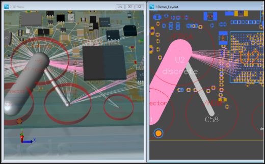
Don’t waste time during floor planning dispersing components at the board edge and dragging them on. With PADS Professional, layout and schematic engineers can quickly create, view, sort, organize, and append planning groups (a hierarchical structure of related components used as a guide during floor planning and placement) to preserve the engineering design intent and guide placement. You can also view the connectivity between groups and components.
The benefits of 3D design
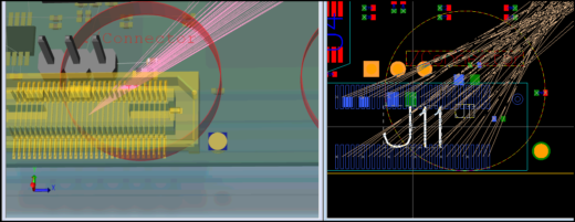
Although designing in 2D is standard operating procedure in most design flows, you can’t design a PCB in isolation; you are designing a system. Use PADS Professional 3D to view how the enclosure mounts to the PCB, for identifying component placement violations, and for presenting a photo-realistic product mockup. A holistic design approach that left shifts design decisions earlier in the design cycle ensures faster time to market, enabling you to catch design issues earlier in the design cycle and run verification checks before the system is physically created or sent out for prototyping.
If you’re looking for efficient design of complex PCBs, take a look inside PADS Professional.
