PCB design best practice: design and manufacturing collaboration

Another best practice to talk about within the digitally integrated and optimized pillar is the collaboration between design and manufacturing and how those two disciplines are exchanging data. This is often called Design for Manufacturing or DFM.
What is Design for Manufacturing (DFM)?
Design for Manufacturing, or DFM, is the design of a PCB with the manufacturing process in mind. DFM is should be considered throughout the design flow. DFM ensures a seamless design-to-manufacturing hand-off.
What’s not working?
In the past, what we’ve seen is that the data that we’re handing to manufacturing doesn’t address producibility or manufacturability. As we throw stuff over the fence (and I don’t mean that literally), I mean that when we hand over poor quality data, that’s not optimized, you end up running into problems, which can then lead to work stoppages because you have technical queries coming back at you indicating that there is an issue or concerns that need to be addressed in order to move forward.
What are the roadblocks?
Roadblocks could include a wide spectrum of design or manufacturing issues. Then, there is the competitive pressure on the fab shop or manufacturing to just accept the data and make their own internal changes – tweaking the design just enough to get the design at a level to move forward with the fabrication. Often, they don’t provide what they tweaked or what they adjusted in the data provided, back to engineering. This potentially prevents teams from optimizing and continuously improving their design as they produce their future designs. Instead, design teams are producing the same stuff, with the same quality or potential issues, over and over. Sadly, this is what is taking place today.
Best practices: design and manufacturing collaboration
Data exchange should be bidirectional. By doing this, we enable lessons learned from manufacturing to be fed back to design/engineering. That bidirectional loop, or that data exchange, has to highest potential to positively influence the design. The best practice in doing this is by utilize intelligent data formats such as ODB++ and IPC-2581. These types of data formats enable intelligent communication from engineering to manufacturing or vice versa. The value we gain is an optimized, integrated bidirectional collaboration that minimizes errors during the data exchange, and it provides a continuous feedback loop of lessons learned back to design/engineering.
How it works: design and manufacturing collaboration
Detailed stackup planning early in the initial design process allows you to optimize your stackup by allowing users to perform pre-layout signal integrity simulations based on the actual materials your fabricators will use.
This allows for calculating single ended or differential impedance as well as insertion loss for microstrip signals, including the ability to add in the effects of solder mask and hatched plane.
After identifying the materials to be used in the design, you can use that information to start building the stackup using a wizard, which will walk you through the construction of a new stackup. Once complete, the stackup information can be exported and sent to the fabricator.
A digital thread between design and manufacturing enables teams to minimize the respins that often happen between the design and manufacturing teams. Streamlining the transition to manufacturing requires sharing a complete understanding of the product and enabling early downstream access to the data.
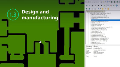
Running a manufacturability analysis before sending to your manufacturer allows users to catch issues before sending their design to their manufacturer, minimizing respins and eliminating the possibility of undesired changes made to the design by manufacturing.
Potential manufacturing issues are easily identified and can be viewed within the tool. A report can also be exported for use in identifying problem areas that need to be addressed in the next revision.
Visit our website or watch this video to learn more about design and manufacturing collaboration.


