are you still verifying your prototype visually?

Are you still verifying your PCB prototype visually?

After completing component placement, it may take months for designer to complete the routing process and finish the entire PCB layout. At this point the CAM data can then be handed out to manufacturers for PCB manufacturing and assembly. After investing this much time and effort, you would probably expect the final prototype to be built as expected, with high quality and reliability.

Practical Manufacturing Standards – Listening to the PCB industry

I love a good story.  Storytelling is the new, cool skill to list on your CV, but listening is possibly…

A poorly validated alternative part is placed on its toeprint

Are your alternative parts well validated before release

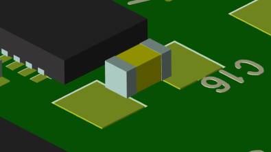
In alternate part selection, many aspects need to be considered: electrical function, physically fit, supply chain flexibility, cost, etc. Every aspect is important during alternative part selection, but realistically, electrical and physical fit are the main prerequisites when choosing a new alternative part. alternative parts well validated

Solder strength testing and validation

Strengthening PCB Solder Connections

To increasing the overall solder strength within a PCB design, designers should be focusing on two distinct but related factors: The material composition of the solder, and the pad and footprint layouts for individual components. The composition of the solder itself will depend upon the application of the board, the components, construction method and materials within the board, and the overall final board quality. The overall footprint of the component will be dependent upon the components within a BOM and the recommended assembly guidelines of your assemblers. Both of these factors rely on discussions and interactions with your assembly house and leaving these discussions until after the design has been released ultimately limits your assembly options.

Exploring Manufacturing Driven Design for automated DFM

Manufacturing Driven Design leverages the intelligence within your PCB Design

Intelligent Process-Driven DFM Analysis for PCB Designers Recent component shortages and distribution disruptions have exposed both the fragility of global…

thin PCB design

What are the advantages and disadvantages of a thinner PCB?

Design for manufacturing (DFM) is an essential aspect of the new product introduction (NPI) process, and PCB design is a…

pick and place machine on PCB SMT line

How to Optimize PCB Design for the SMT Assembly Process Flow

PCB (Printed Circuit Board) design layout optimization is critical for the success of SMT (Surface Mount Technology) assembly. SMT assembly involves placing surface mount components directly onto the surface of the PCB, as opposed to through-hole components, which require holes to be drilled through the PCB. SMT assembly is faster, more precise, and more cost-effective than through-hole assembly, but it requires careful design optimization to ensure a successful assembly process.

Migrating from Gerber to ODB++ CAM Compare

Gerber files have long been the industry standard for PCB design and manufacturing data. However, with the increasing complexity of modern designs, Gerber files have become less effective in conveying all the necessary data required for manufacturing. ODB++ is a newer format that was developed specifically to address the shortcomings of Gerber files. ODB++ is a comprehensive format that includes all the necessary data for manufacturing, including component placement, drill files, and manufacturing details such as the thickness of the PCB and the type of solder mask just to mention a few.

AOI image

Manufacturing Driven Design – Taking DFM to the Next Level

Manufacturing Driven Design (MDD) is an evolutionary approach to DFM. It enables the effortless exchange of manufacturing process constraints so that an OEM can assess the manufacturability of a design in perfect alignment with their supplier