Ensure PCB reliability with structural analysis using a calculated thermal map

Managing thermal challenges of complex multi-layer PCBs
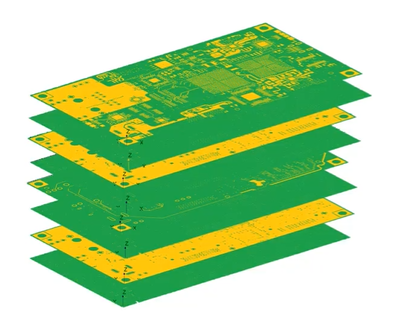
Electronics and semiconductor companies face increasing market challenges from complexity, new technology adoption and new market drivers. The complexity arising from miniaturization, increasing functionality, and tighter electronics systems integration can require complex multi-layer printed circuit boards (PCB) with upwards of 50 layers.
These multi-layer boards present electrical, thermal and mechanical challenges for designers, especially when used in mission-critical applications such as in the medical field, data storage, satellite systems, 5G, high-performance computing (HPC), machine learning (ML) and artificial intelligence (AI). Better prediction and understanding of physical product performance and assessing reliability earlier in development are critical to overcoming these challenges. Developing complex market-leading products faster requires an innovative engineering approach.
Benefits of using simulation and test for structural integrity to develop more reliable PCBs
Assure the structural integrity of electronics components and systems at an earlier stage in the development lifecycle via combined insights of test and simulation:
- Identify high-stress areas: optimize design where needed, reduce material
- Integrate CAD and CAE: unified design and simulation environment
- Verify vibration standards: vibration qualification and structural testing
- Reduce thermomechanical fatigue: increase field lifetime
Deciding when to use what type of thermal modeling may challenge some designers as they balance computational time over benefits.
Reviewing PCB thermal modeling approaches
The four PCB thermal modeling level approaches require different inputs, offer different information and are useful at different phases of design.
- Level 1: Compact Phase (pre-layout) – Useful for making architectural choices at early, conceptual stages of design.
- Level 2: Detailed/Layered Phase (layout verification) – Allows for more accuracy in calculating heat spreading in layers.
- Level 3: Material Map Phase (layout verification) – The material map is a special case of the printed circuit board defined by the local characteristics on the uniform grid for each board layer and takes into account effective density, thermal conductivity, etc.).
- Level 4: Explicit Copper Phase (final verification) – Direct modeling of copper in selected areas or on the full board including layers and vias.
Because Level 3 uses “averaging” representation, it needs less physical memory (RAM) and computational time. The PCB is still modeled as a stack of layers and is useful for designers to leverage as part of a new approach.
Leveraging the SmartPCB Material Map approach for PCB reliability
 The SmartPCB material map approach is a new technique to accurately model the complex copper traces within the printed circuit board without the significant computational overhead. The simulation model is a thermal network generated using EDA data while avoiding the need to convert EDA data into a CAD model explicitly.
This approach enables:
- Electro-thermal co-simulation to reduce costly design re-spins, ensuring the reliability of the board and components and accelerating product design.
- Structural analysis of the PCB using the calculated thermal map, ensuring mechanical reliability of the product
Learn about the unique SmartPCB approach to simulate thermal, thermo-electrical and structural phenomena of the printed circuit board in this on-demand webinar. The presenter demonstrates combined electro-thermal co-simulation to account for self-heating in higher power applications and thermo-mechanical analysis workflows to improve result accuracy and increase design productivity.