Chip production and design with 3D IC technology


The semiconductor industry has long relied on Moore’s Law, the observation by Intel’s co-founder Gordon Moore that the number of transistors on a chip doubles every two years, and the performance of the chips doubles as well. That’s been happening for the last 60 years, but as we reach the physical limits of transistor miniaturization, the rate of progress has slowed. The industry needs innovative solutions to continue delivering the powerful computing platforms that our digital world demands. That’s where 3D IC technology comes into play.
What is 3D IC?
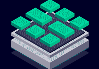
Rather than building ever-larger and more expensive monolithic chips, 3D IC (3D integrated circuit) allows us to package multiple smaller chips together in a single package. This approach leverages existing technologies and manufacturing processes that are already optimized for efficiency and yield. By interconnecting these chiplets in a 3D stack, we can achieve higher performance and lower power consumption without the limitations of having to rely on ever smaller transistors.
Our comprehensive 3D IC solutions
We recognize the potential of 3D IC to remove the limits and revolutionize semiconductor design and manufacturing. Our comprehensive portfolio of software and services provides the key enabling technologies for 3D IC adoption. Siemens EDA offers advanced 3D IC design tools that allow engineers to efficiently layout and interconnect multiple chips in a single package. These tools, such as Xpedition Substrate Integrator and Xpedition Package Designer, streamline the 3D IC design process and enable faster time-to-market.
Mechanical design and thermal management
But 3DIC is not just an electronic design challenge – it also requires innovative solutions in mechanical packaging and thermal management. This is where Siemens’ mechanical design software, NX, comes into play. With NX, engineers can design and simulate the complex mechanical structures needed to house 3D IC modules without creating thermal issues.

Thermal management is critical for 3D IC performance and reliability. Our Simcenter portfolio provides the advanced simulation capabilities needed to analyze and optimize the thermal behavior of 3D IC designs. By leveraging multi-physics simulation and multi-objective optimization, engineers can ensure that 3D IC modules operate within safe thermal limits while maximizing performance.
Semiconductor lifecycle management
What sets Siemens apart is our ability to bring all these pieces together to solve the complex, multi-domain challenges of 3D IC design and manufacturing. No other company can provide such a comprehensive set of solutions spanning electronic design, mechanical engineering, and advanced simulation. Our Semiconductor Lifecycle Management solution enables customers to effectively manage the engineering processes and bill of materials (BOM) structures associated with these increasingly complex IC packages. By streamlining data management and collaboration across the entire semiconductor lifecycle, we help our customers navigate the intricacies of 3D IC technology with greater ease and efficiency. We are uniquely positioned to help our customers adopt 3D IC technology and drive the next era of semiconductor innovation.
Learn more
To learn more about how Siemens is enabling 3DIC design and manufacturing, visit:
- Siemens EDA: Designing 3DICs with Xpedition
- Siemens NX: NX for the Semiconductor Industry
- Siemens Simcenter: Simulating and Optimizing 3DIC Designs
- Siemens Semiconductor Lifecycle Management: Three solution tracks.
At Siemens, we’re committed to providing the innovative, sustainable solutions that our customers need to overcome the challenges of semiconductor design and manufacturing in this new era of 3DIC. Let us help you bridge the gap between chip production and design and unlock the full potential of 3DIC technology.
For more about 3 DIC, watch my interview here.


