Connecting PCB developers to fabricators to saving them time and money; the Nistec experience

At Siemens, we’re always talking to electronics designers. And not just the ones that work at technology giants – but also the ones that work for small and medium sized businesses. The designers at small-to-medium sized enterprises (SMBs) have to work differently than their “big” brothers. They have fewer tools, and have less access to in-house expertise on the manufacturing process.
Because of these limitations, the handoff from design to production can take longer at SMBs — more design spins, more trial and error, and more discussions with the fabricator about the fab’s capabilities and limitations. The designer relies on the manufacturer to perform DFM analyses and error checks – sometimes in 2, 3, or more cycles. The process can take weeks, and in complex scenarios, perhaps months. This is critical time wasted, as the developer is forced to wait before starting to test and deliver the product.
Understanding this problem, we’ve been working on a new tool – an easy-to-use, on-line collaboration space that will help SME designers greatly accelerate the design-to-manufacturing process.
How PCBflow’s DFM process works
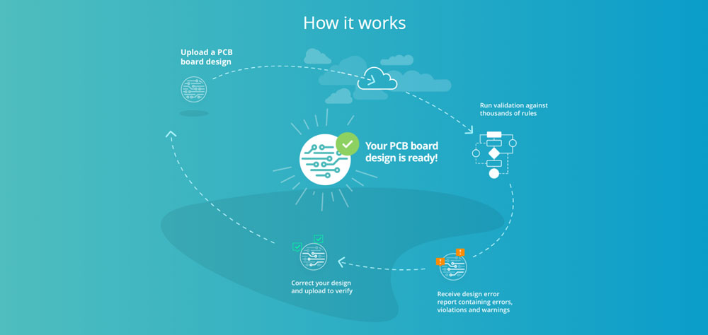
Instead of receiving designs and spending time and effort on debugging them, the manufacturer simply uploads their fab’s “DFM profile” to the space. The profile contains secure data on their fabrication capabilities and limitations. Then, the designer uploads the design to the space, and runs a DFM analysis using the fabricator’s profile and set of constraints. The DFM analysis report is issued within seconds, listing all the issues that require handling to make the board manufacturable. Thus the designer can independently revise the design until it is ready to be submitted to the fabricator – with no need for additional spins. Once the file is received, the fab can immediately give the developer a quote – without having made a single phone call or site visit. No time wasted analyzing the design.
In addition, this collaborative space helps connect between fabricators and potential new customers – helping them to improve conversion rates while investing less time and effort. Communications barriers resulting from differences in time, location, and language, are easily overcome.
The process of developing this tool was greatly enhanced by the contribution of our customer, Nistec (www.nistec.com), who collaborated with us on this project. Nistec happens to be both a board designer and a manufacturer – they understand the difficulties experienced by both sides. So I’m particularly grateful to Evgeny Makhline, Yaron Snir, and their team of professionals who helped us to pinpoint the major challenges in the industry, allowing us to close the gaps and accelerate the tool’s development progress.
Evgeny Makhline, Nistec’s CTO told me, “This is a great idea that’s a win-win for board designers and for fabricators. On one hand, board designers get easy access to a cost-effective, easy-to-use platform that quickly identifies design issues and constraint violations that could affect manufacturability, and then connects them with a wide variety of fabricators. The fabs, on the other hand, receive a ‘mature’ design that requires little or no review or troubleshooting – a big savings in time and material.”

Sign up and try PCBflow for free at www.pcbflow.com
This article was written by Yossy Pinhas, who is the Product Manager responsible for the PCBflow platform in Siemens.


