Managing the complexities of High Bandwidth Memory integration in high-performance computing

The utilization of High Bandwidth Memory (HBM) has become a cornerstone for high performance computing (HPC) CPUs, GPUs, and AI applications. However, High Bandwidth Memory integration poses significant challenges for package designers, stemming from its unique architecture and stringent performance requirements. Let’s delve into the intricacies of High Bandwidth Memory integration methodologies and explore how innovative approaches are tackling these hurdles.
High Bandwidth Memory features a 1024-bit bus divided into channels, typically structured as either 8 x 128bit or 16 x 64bit configurations.
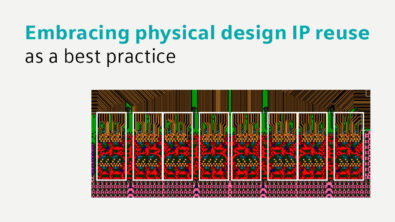
The initial step in High Bandwidth Memory integration involves creating complex via geometries for fanout/breakout structures. These structures facilitate routing the bits of the channel from complex via breakouts on the logic die side to the breakouts on the HBM stack. Once the initial channel is completed and characterized for electrical compliance, it serves as a template for replication and reuse across the memory stack.
However, the dynamic nature of compute chiplets or Systems-on-Chip (SoCs) often necessitates refinement, impacting die bump or pin assignments. Modifying a part of an existing replicated channel to reflect these changes can lead to time-consuming engineering change orders (ECOs). This is where innovative solutions like Physical Design Reuse Circuits (PhRC) come into play.
Physical Design Reuse Circuits (PhRC)
PhRC enables intelligent circuit replication, supporting dynamic propagation from the parent netlist to facilitate rapid ECOs and management of the golden source netlist. By leveraging PhRC, design teams can achieve significant time savings, with potential reductions of up to 25% in total integration time over conventional methods. When combined with automated ECO processes, these savings can soar to as high as 75%.
Challenges faced by semiconductor package designers
High Bandwidth Memory integration not only requires technical prowess but also demands a strategic approach to address the multifaceted challenges. Designers must balance performance requirements with efficiency and flexibility to adapt to evolving design iterations. The challenges faced by package designers can be broadly categorized into four key areas:
- Maintaining signal integrity is paramount in High Bandwidth Memory integration, given the high-speed data transfer involved. Advanced signal integrity analysis tools and techniques are employed to mitigate signal degradation and ensure reliable data transmission.
- Ensuring power delivery stability is another critical aspect, as HBM requires consistent and robust power delivery to meet performance specifications. Careful power distribution network design and optimization are essential to minimize voltage fluctuations and ensure stable operation.
- Managing routing real-estate efficiently: Efficient utilization of routing real-estate presents yet another challenge, particularly in densely packed designs where space is limited. Optimized routing algorithms and layout techniques are employed to maximize routing efficiency while minimizing signal crosstalk and interference.
- Meeting design cycle time constraints is a perpetual challenge in HPC development, where time-to-market is critical. Agile methodologies and automated design workflows are leveraged to streamline the integration process and accelerate time-to-market.
High Bandwidth Memory integration presents unique challenges for package designers in the realm of high-performance computing. By adopting innovative methodologies and leveraging advanced design tools and techniques, design teams can overcome these challenges and unlock the full potential of HBM in next-generation computing systems.
Read more about this concept in our eBook: IC Package physical design best practices


