So far in our 3D IC blog series, we’ve discussed efforts to create chiplet ecosystems, design workflow changes needed to…
Part 1: An advanced IC packaging design and verification solution For many applications, next generation IC packaging is the best…
With current 3D IC packaging technologies, since the system-level netlist (the 3D IC design intent) drives system-level LVS verification, designers…
Over last 2-3 years, everyone has been talking about Moore’s “Law” becoming invalid. Even if it does, we will continue…
In our last blog about 3D IC, we discussed the models chiplet vendors need to provide System-in-Package (SiP) integrators to…
Semiconductor engineers aim to deliver best-in-class devices despite technology scaling and cost limitations of monolithic integrated circuit (IC) design. To…
In the first podcast about 3D IC heterogeneous integration, we talked about the disaggregation of once monolithic implementation architectures into…
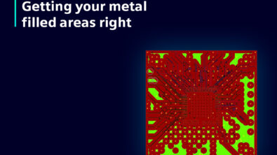
If you’re involved in semiconductor package design using routable substrates — that is, as opposed to leadframe based — then…
As consumer electronic devices grow increasingly connected, intelligent and advanced, designers need new methodologies such as 3D IC to address…