Revolutionizing Electron Microscopy: Semplor’s Desktop SEM
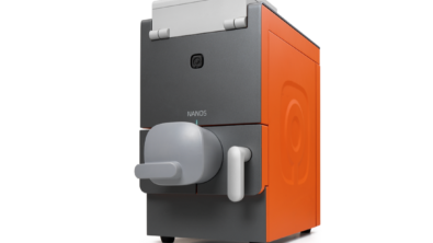
Traditional scanning electron microscopes (SEMs) are large, expensive, and complex pieces of lab equipment. To use, maintain, and repair them requires specialized knowledge and skills that few companies and research institutions possess. This challenge encouraged Semplor to revolutionize the field with their innovative product, NANOS—an easy-to-use SEM the size of a desktop computer.
“Anybody, anywhere in the world should be able to work with SEMs, that’s our goal,” says Emile Asselbergs, CEO and co-owner of Semplor. “Like a modern cellphone, you don’t need a training course to use them. It’s easy, fast, and doesn’t break.”

Rethinking SEM Technology
The Netherlands-based company achieved this paradigm shift by rethinking SEM technology and designing the NANOS from the ground up. However, as a small startup, Semplor didn’t have the budget for most engineering design software.
“We contacted Siemens Digital Industries Software and Enginia and asked if they could help us,” said Asselbergs. “With Enginia we were in contact about the Solid Edge Startup Bundle. They provided us with Solid Edge software, which was mostly free of charge for two years, and assisted with the license installation and demonstrated how to use the Solid Edge Standard Parts Library. We designed the entire system with the program from Siemens.”
As a result, Semplor transformed the traditionally complex SEM into a machine that fits seamlessly into any startup, SME, makerspace, or big-name research lab.

Simplifying Complexity
Asselbergs explains that traditional SEM equipment can be hard to maintain. “You open them up, and they are large, complex, with lots of circuit boards. It needs a lot of maintenance.”
While working in the SEM field, Asselbergs and a few colleagues realized that the equipment doesn’t have to be this complicated. “We’ve been thinking about how to ideally design a tabletop SEM. We didn’t use the things of the past or things we didn’t like; instead, we made a new concept,” he says. “Organizations have difficulty changing mindsets. That is what we love to do.”
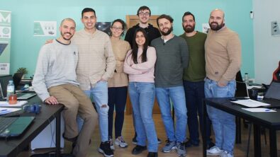
Asselbergs’ colleagues soon became co-founders with a shared goal: to use their combined 200 years of experience with SEM to democratize the field. They understood the common user pain points and wanted to build something better. “It’s what people need these days; when you have a problem, you want to solve it now.”
User-Friendly Interface
Aside from the physical design of the NANOS, its software user interface also plays a big role in simplifying SEM. The UI has many automatic functions to optimize brightness, contrast, and illumination. It also guides the user through the process so that those who are new to SEM can catch on quickly. However, it also contains many of the power-user features used by seasoned veterans in the field.
An example of how the NANOS democratizes SEM can be seen with how it deals with living samples. These samples contain a lot of water and are sensitive to the beam of electrons. Traditional equipment overcomes this challenge by coating living samples in gold, platinum, and other expensive materials. Newer SEMs offer the option to operate at low vacuums, which ensures that living samples don’t shrivel and the charge they experience is neutralized. For the NANOS, this feature comes standard without added expense.
“We don’t use vacuum gauges, just good calculations,” says Asselbergs. “By the pump power and RPM, we know the vacuum level. Measuring gauges cost money and can break, so that’s something we don’t want to use.”

Highly magnified views of various objects in the NANO electron microscope
Maintaining Functionality While Simplifying
Scrapping the vacuum gauge demonstrates the strategy Semplor used when designing the NANOS: If it’s not there, it can’t break or take up space. This enabled the design team to reduce the size of the SEM while also improving its reliability.
This philosophy sets the NANOS apart from other tabletop SEM devices. “They are basically low-end systems and look like a large microscope shrunk into a smaller one. They are very traditional when you open them up,” Asselbergs explains.
However, simplifying the traditional SEM design doesn’t mean the NANOS is short on advanced features and capabilities. The redesign enabled Semplor to develop new features and future-proof the final product.
For instance, the NANOS contains an eucentric stage that keeps the sample in focus as it’s tilted. This feature ensures that every sensor currently aimed at the sample remains aligned and focused. In traditional equipment, tilting the sample would require the user to change SEM settings to refocus the sample.

The Role of Engineering Software
The main design team on the NANOS consisted of one physicist and one mechanical engineer. They received help from Siemens, Siemens Partner Enginia, and even Semplor’s manufacturing partners.
“The system was designed and engineered with the people that would manufacture the system,” says Asselbergs. “We knew what they had in terms of manufacturing machines and based on that knowledge we designed the system for them to manufacture and assemble.”
Solid Edge was used to track the design, manufacturing, and building logistics. This ensured all stakeholders, internal and external, were aligned. “We do nothing on paper,” says Asselbergs. “You talk to many suppliers and can have a meeting five minutes long without being in the same physical spot. Many suppliers have CAM systems to operate machine millings and lathes and it’s been my goal to work with those suppliers without making 2D drawings with tolerances.”
The 3D models made in Solid Edge also helped Semplor ensure that the NANOS was easy to maintain. For instance, designers were able to ensure that parts could be easily accessed and changed out. “It helps if you have a good 3D model of your system to assess if parts are easily accessible,” says Asselbergs. “We knew the system before we built it. If a PCB breaks, the user untightens four bolts and a few connectors, puts in the new PCB, and sends the old one in for a refund. You can replay this maintenance in Solid Edge to make sure it works, is easy, and is optimized.”

Solid Edge didn’t just simplify the maintenance, logistics, prototyping, and manufacturing of the NANOS, it also reduced the number of physical prototypes needed via simulations. Part stiffness, modal vibrations, and other mechanical assessments were done in the software. Meanwhile, many of the field calculations and electron beam simulations were made using separate academic software and in Solid Edge.
“A lot of simulations were done before parts were made,” says Asselbergs. “We looked at 10 different setups to optimize the design.” Regarding Solid Edge, Siemens, and Enginia specifically, Asselbergs adds, “they helped us design the system to work on the first go. We’re very happy with it.”
To learn how Solid Edge can help the development of your product, learn more here.