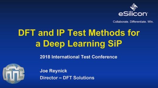
eSilicon Masters DFT and IP test for a deep learning SiP with Tessent
eSilicon used the Tessent family of DFT solutions to solve their toughest challenges of testing a large 2.5D/3D deep learning device. Hear all about it in this 15 minute video.
With over 300 tapeouts, there is no doubt that eSilicon has tons of experience getting designs done. So when Joe Reynick, Director of DFT solutions at eSilicon describes their DFT strategy, it’s probably worth a listen.
 Reynick says that they use Tessent to solve the issues affecting DFT (memory BIST, scan, boundary scan) and IP test (SerDes loop back, PLL test, etc.), for their large 2.5D/3D device. The application of hierarchical DFT and IP test is the focus of this presentation by Reynick, recorded live at the 2018 International Test Conference.
Reynick says that early DFT planning is key, even as early as the sales phase, because so many factors affect the DFT strategy. They start early with the basic DFT plan and build on it as more information becomes available. They needed a DFT platform that was comprehensive and flexible to accommodate an evolving DFT plan throughout the design process.
They use IJTAG for chip and IP testing. This allows eSilicon to deploy IP with the IJTAG files so the end users can generate test vectors at the top level. With IJTAG, users do not need to figure out the tests themselves based on a Verilog test bench.
For this 2.5D deep learning device, eSilicon implemented new flows like IO BIST and lane repair inside the package. They are seeing very few IOs available for test at the package pin-level. SerDes are taking over the large parallel busses. Tessent hierarchical DFT and IP test solves all the issues and challenges eSilicon faced with this project.
The hierarchical DFT methodology allowed them to test smaller chunks of the chip at a time and sped up the turn-around time for debug. Testing smaller pieces of the design at a time also helped control the test power.
Reynick goes into deeper look at the 2.5D/3D deep learning device architecture and describes the DFT and IP test requirements. He also describes the DFT verification, simulation of test vectors, test power control techniques, and use of an ATE for bring-up/debug.
“Hierarchical DFT speeds up all processes,” says Reynick. “I can’t emphasize enough how much you should be doing hierarchical DFT if you’re designing over 2000 flops/chip.” They saw significant yield improvement, 30% from memory repair, and they got very high test coverage. For the AI portions of the chip, they used testpoints to reduce test vector count. Finally, during first-silicon bring up all DFT tests passed within 4 days.
Watch the 15-minute video here to hear more details about the work eSilicon did and how Tessent helped them with all the test challenges of their large finFET device.


