DFT for AI chips draws a crowd at ITC India tutorial
At the recently concluded ITC India conference, Mentor experts presented the two highest-attended tutorials. One tutorial was AI Chip Technologies and Its DFT Methodologies, presented by Mentor’s Yu Huang, Rahul Singhal, and Lee Harrison
Hardware acceleration for Artificial Intelligence (AI) is now a very competitive and rapidly evolving market. There are more than 50 startups and 25 established semiconductor companies all racing to capture a portion of the business.
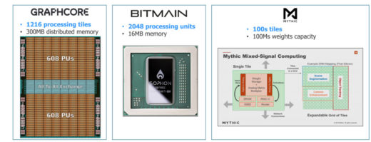
The ITC India tutorial covered the basics of deep learning and gave an overview of how AI chips accelerate deep learning computations. They covered the critical and special characteristics and the architecture of the most popular AI chips. For example, the chips being created by startups like Graphcore and Mythic are creating ASICs based on the novel, massively parallel architectures that maximize the data processing capabilities for the AI workloads. The new AI chips are typically very large, complex, and use leading-edge process technologies. While the architectures vary, they share a few key design characteristics, such as:
• Very large designs with billions of gates
• A very large number of replicated processing cores
• Distributed memories

The presenters discussed how the AI chip architectures influence the DFT implementation strategy and why the traditional design-for-test (DFT) approach for full-chip flat ATPG breaks down when applied to AI chips. They defined three key strategies that work towards a time-to-market goal for AI chips:
• Exploit AI chip regularity
• Insert and verify DFT at the register-transfer level (RTL)
• Eliminate DFT-to-test iterations during silicon bring-up
The presenters introduced the DFT technologies that are targeted to the testing of AI chips with the goal of speeding up time-to-market. Most important is having a true hierarchical DFT flow, in which the DFT implementation, ATPG, and scan test pattern verification are performed at the core level. That is, sign-off is only performed once for any given block, then that signed-off block can be replicated to any number of instantiations at a higher level of the design. SoC design teams who adopt hierarchical DFT have seen up to 10x faster ATPG with 2x pattern reduction and radically accelerate bring-up, debug, and characterization of AI chips.
DFT tools like Tessent also save time by inserting test logic in RTL instead of at the gate level. RTL simulation and debug are much faster with RTL, and change iterations can be completed before time-consuming synthesis. RTL insertion of DFT also allows for early I/O and floor planning.
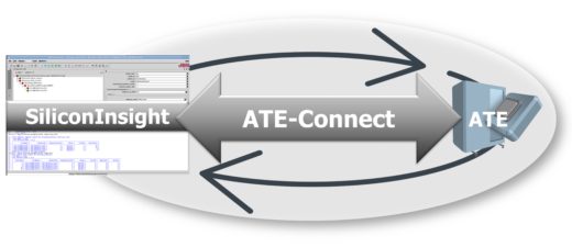
To eliminate DFT-test iterations, a new technology that connects the ATE and DFT environments (called ATE Connect), lets the DFT engineers drive the silicon bring-up. The AI chip company, Graphcore, adopted this solution for silicon bring-up and also for complete testing of their parts. They completed silicon bring-up within three days and shipped fully tested and validated parts within the first week, far ahead of schedule.
The presenters showed the Graphcore results along with a few other case studies that demonstrate the value of using DFT technologies specifically tailored to the needs of AI chips.
If you missed the AI chip tutorial, you can still read about how Mentor approaches DFT for AI chips in this whitepaper.


