How do you do PCB Stackup Planning?

Planning for Signal Integrity
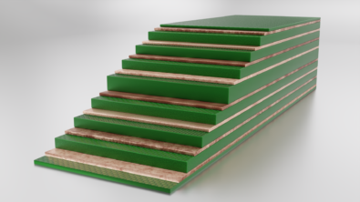
Stackup planning is one of the most important but often overlooked aspects of a successful PCB design. Selecting the right dielectric material and stackup properties to meet the performance characteristics of the design is crucial to the products success. Choosing the incorrect material can lead to excessive electromagnetic emissions, crosstalk, and other signal integrity issues. Selecting the correct materials and stackup can help you reduce the design cycle time which leads to reduced costs as well as improved fabrication of the PCB.
There are many ways to accomplish stackup planning. Let’s look at a few of the different way’s companies handle this process.
Some companies use the trial-and-error method. Once a stackup is proven to work it is used repeatedly for all new designs. Obviously, this method is not cost effective at all. It also doesn’t lend itself to optimizing the materials for the specific design characteristics.
Impedance Controlled Design
Other companies rely on their fabricator to perform their stackup planning for them. This method could be called “Impedance Controlled” design. This is where you indicate to the Fabricator that certain line widths on “X” layers must meet a specified impedance and the Fabricator must supply test results to prove the impedance requirements were met. This seems to be the most common way stackup planning is done today. At some level this makes sense since the fabricator knows what materials they have in stock and how their fabrication process works to assure the stackup meets the impedance requirements. Unfortunately, if the design is moved to another vendor or is sourced from multiple vendors there can be quite a difference in how the stackup is constructed.
Impedance by Design
There are other companies that take total control and ownership of the stackup. This method could be called “Impedance by Design”. Knowing all the various tolerances and the materials properties assures that when your design is built to spec the impedance needs will be met. Owning the stackup is important in making sure that the PCB fabrication is consistent not only at one vendor but at every vendor for the life of the product. For example, by using a tool such as Z-planner Enterprise, all aspects of the stackup can be modeled and thoroughly documented so there is no confusion or misunderstanding with your fabricators.

Dielectric Material Library
Using a tool such as Z-planner Enterprise allows you to create the correct routing rules by performing impedance and insertion loss analysis prior to layout. Also having a vast library of dielectric materials allows you to compare the performance of these different materials using your design goals. If you have several different materials that will meet your needs, you can easily document them and send them to your vendors for availability and quoting purposes.
Being able to quickly qualify materials based on your known electrical tolerances, and not upon the materials availability of your selected fabricator is key for efficient stackup design. This allows you to optimize the design around the available materials and take complete control of your stackup.
Seamless Integration
Another benefit of owning the stackup planning process is the ability to drive the stackup into your other tools including your ECAD (Electrical Computer Aided Design) and SI (Signal Integrity) tools. Having the ability to seamlessly import and export the stackup reduces any chance that a translation error will be present. All the impedance and insertion loss routing rules will be well documented and available to be archived with the rest of the design data.
Owning and controlling the stackup will increase the knowledge base of the design team, which in turn will lead to better and more robust designs. Hence, “Impedance by Design” is less expensive than “Impedance Controlled” design.

