Why is Design for Manufacturing important?
Who is PCB DFM for?
For those of us that have climbed a mountain to take in the gaze of a magnificent view from the top, only to find the view obscured by a thick haze. For those of us that desperately needed to go to the grocery store, only to discover once there they had forgotten their list on the kitchen counter. For those of us that have broken a glass, swept up the mess and minutes later find a small shard ready to be stepped upon. These are all illustrations showcasing why design for manufacturing during the PCB layout process is needed and how unexpected and unintended outcomes can happen to good people.
Design for manufacturing validates PCB design readiness and results in a PCB manufacturing process with no known conditions that negatively impact time to market, ensures that no manufacturing process requirements are left overlooked, and that yield is never impacted by even the smallest of conditions. Let me briefly illustrate.
Work within your PCB manufacturing capability
- Begin by involving the manufacturers that are going to produce the PCB early, while at the same time automatically begin evaluating the layout against the manufacturer’s process capabilities. It is not uncommon for a prototype of a design to be validated, only to have a small final change alter a process requirement, requiring additional design re-spins and ultimately adding additional time to the product realization outcome. Identifying these issues early maximizes the return on your next New Product Introduction.

General spacing checks like an Under Bump Metallurgy (UBM) check are important as insufficient pad design may cause soldering bridging during the manufacturing process. In this instance the red range of requirement is 12 mil, but the measured spacing is 6.7 mil, thus the feature is flagged and given a severity level of red: unmanufacturable based on current manufacturing capabilities.
Perform a PCB process review
- The ideal drill aspect ratio for through holes is 10:1 and for microvias is 0.75:1. Not adhering to such a ratio means that the plating process on the wall of the holes, which connects the layer together in the Z-axis of the board, will not be properly formed. It is not uncommon for a design to reach manufacturing only to find that the PCB drill depth over the drilled diameter was not considered as part of the PCB DFM process requirements.

The capability of microvia analysis of Valor NPI is not only for vias in same layer and same net, but also for vias in different drill spans and different nets.
Design to increase your PCB yield
- Ceramic capacitors when placed to close to the edge of a board is a condition prone to a yield disaster. Components in all cases need to be kept a certain distance from the edge of the board to protect yield. As board space becomes denser with components, the need to follow PCB DFA process requirements becomes has become more critical than ever before.
Explore Valor NPI with our Online Trial
Explore Valor NPI with our free online trial and find out how easy it is to implement the world’s most advanced DFM software. With no download or installation necessary, this simple guided tour provides immediate hands-on experience. Select your desired workflow:
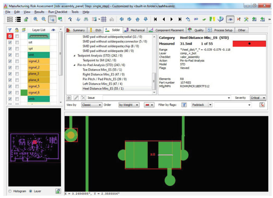
Design for manufacturing process requirements
When properly executed, design for manufacturing with Valor NPI will ensure process capabilities are easy to follow throughout the layout process, enabling the final product to achieve the time to market expectation. The results of adhering to process requirements will optimize the manufacturing portion of the product realization process. Finally, following process requirements will automate the detection of what might be the smallest of all manufacturing oversights that would result in additional costs, a reduction in yield and poor reliability in the finished product.
