No One Expects Gate Level CDC Verification and Glitch Detection for ASIC Signoff!
[Preface: at the upcoming DVCon 2018 in San Jose, poster 4.12 addresses some of the issues raised below, as well as DVCon San Jose 2017 paper 12.3]
There you are, satisfied that all of your tape out criteria were met: at the RTL level, every form of “coverage” you could think of was applied, and 100% coverage scores were achieved across-the-board. Similarly, your RTL clock domain crossing (CDC) verification was clean. At the gate level, all the gate-level simulations (GLS) passed with flying colors, and weeks of static timing analysis (STA) came to a successful close.
Yet here you are in the lab, hovering over samples that keep rebooting at seemingly random intervals since you first powered them up.
“Why do bad things happen to good people?”
“Why is this happening to ME?”
“I wasn’t expecting any errors or glitches …”
<<< CUE DRAMATIC ENTRANCE MUSIC >>>
Sadly, this classic comedy reference is no joke for many of our customers: recently one D&V team found themselves in this exact situation, where samples of a chip destined for safety-critical applications was periodically hanging. Clearly the customer’s customers would never accept such a device, and the window for their acceptance was rapidly closing. Bottom-line: if the re-spin didn’t work, the sockets would be lost.
So what can be done in this situation (and/or what did the aforementioned customer do)?
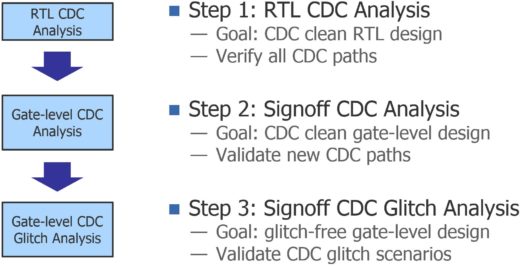
The solution lies in 3 steps, summarized by the following diagram:
Step 1: Make Sure RTL CDC is Clean
First, CDC verification at the RTL level should be completely “clean” before doing any gate level analysis. In short, all waivers should be understood and reviewed by two separate engineers, and the synchronizer choices should be further validated for robustness with a dynamic CDC analysis that includes simulations with behavioral metastability models. The reason for this is relatively obvious: while RTL CDC verification of a large design can be a challenge, at least at the RTL level you can more easily see the relationships between the design and the verification results. But once the RTL is transformed into zillions of gates by a synthesis tool, it becomes much harder to sort through “bit blasted” logic, let alone the various signal name and topology changes.
Step 2: Make Sure Gate Level CDC is Clean
If RTL CDC verification was clean, wouldn’t the chip be safe from any further CDC issues? Unfortunately, no. New, chip-killing CDC error paths and glitches can be introduced on signal paths that were perfectly safe at the RTL level. Rephrasing, if you think you are “safe” because the RTL CDC analysis was successful, you are actually still at risk. While this can happen at relatively “big” nodes, in general our customers’ experiences suggest these effects become a really big threat starting at 28nm and below. To greatly oversimply, the 28nm node seems to be the point where devices “run out of bandwidth” and expose more 2nd order effects like this.
Fortunately, the DVCon 2017 paper 12.3 “Accelerating CDC Verification Closure on Gate-Level Designs”, by my colleagues Anwesha Choudhury and Ashish Hari describes these issues in more detail, and shows how an exhaustive, formal-based gate-level CDC analysis provided by Questa Signoff CDC can eliminate these problems.
Step 3: Run an exhaustive, formal-based, gate-level glitch-detection analysis
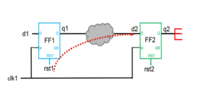
Unfortunately another round of CDC analysis at the gate level isn’t enough: as noted above, glitch detection is also needed since synthesis can also introduce glitch-y signal paths. This typically occurs in-and-around the “de-mux” logic between clock domains and synchronization logic, or the synthesis tool itself inadvertently disrupts the synchronizer logic by being overly aggressive in applying optimizations.
As you might imagine, finding these glitches among 100’s of millions of signal paths and gates is like finding a needle in a haystack. As Jackie Hsiung of Mediatek Inc., and my colleagues Sulabh Kumar Khare and Ashish Hari describe in the upcoming DVCon poster P4.12 “Preventing Chip-Killing Glitches on CDC Paths with Automated Formal Analysis”, they show how an automated formal approach, combined with advanced heuristics, has been delivering “low noise” results on seven real world-SoCs projects.
The happy ending to this whole sketch is that the above 3 steps work in the real world. In the case study mentioned at the beginning, the customer used Questa Signoff CDC to find 3 glitches among millions of signals. One of the glitch sources found was one that they had suspected; but the other two were a complete surprise. The requisite ECOs were implemented, the design was re-verified from end-to-end, and the re-spun samples worked perfectly! (And these engineers no longer fear menacing, red-robed characters bursting into their lab unannounced.)
Until we meet at the upcoming DVCon, may your CDC paths be properly synchronized, and your signaling be free of glitches.
Joe Hupcey III,
for the Questa CDC team
Reference links:
Questa Signoff CDC product overview
Video of the classic Monty Python “Spanish Inquisition” sketch
Comments
Leave a Reply
You must be logged in to post a comment.


Good article, and it’s always nice to have a set of suspenders in case your belt fails. #GateLevelSimulation may catch some of these cases, but by no means can it be expected to encounter all of them. However, I do question one statement by the author:
“the synthesis tool itself inadvertently disrupts the synchronizer logic…”
Why would you ever allow this to happen? All synchronizers should be “don’t touched” and given placement constraints in the layout so the components aren’t separated. No disruption of synchronizer logic is then possible.
Jerry: thanks for your comments! I agree it’s rare a synthesis tool would break a synchronizer, but it can happen if the user isn’t careful with the setup & follow-up. More commonly what we’ve been seeing is glitches slipping through synthesis.