Significantly Improve Your FPGA Design Reliability by Using Custom CDC Synchronizers
[Preface: we are presenting a paper on this topic at the upcoming SEE/MAPLD conference, May 21-24, 2018 in La Jolla, CA – Join us!]
Today’s FPGA designs include multiple cores, interfaces, test logic, and even different internal power and voltage domains. In particular, the multiple asynchronous clocks, and the signals crossing between asynchronous clock domains, may result in functional errors. Specifically, when a signal from one asynchronous clock domain is sampled by a register on a different asynchronous clock domain, the setup/hold timing requirement will be violated for the destination register. This setup/hold timing violation means that the destination register will probably become metastable, so the destination register will settle to an unpredictable value and cause a functional error. To address this, FPGA designers add synchronization logic to prevent the propagation of metastable events.
However, the standard “2 D flip-flop” synchronizer might not always do the job, especially if common pitfalls in positioning the synchronizer in the circuit aren’t avoided. The negative effects are only compounded when the FPGA is going into a challenging operating environment (e.g. continuous exposure to high radiation in space). Consequently, any resulting CDC errors that slip through can lead to intermittent failures that may only manifest themselves in specific operating conditions that may not come up in the lab, and would only be found in certain field conditions. Fortunately, there are easy and effective solutions …
The Common 2 DFF Synchronizer vs. a “Custom Sync”
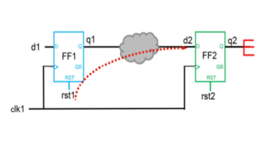
The simplest synchronization structure is a “2DFF” synchronizer (Figure 1 below) – literally two D flip-flops in a row. Unfortunately, designers often mistakenly drive this synchronizer with combinational logic (Figure 2). The result is that the combinational logic will transmit any glitches into the synchronizer, thus reducing the mean time between failure (MTBF) of the synchronizer; and hence the reliability of whole circuit. These CDC mistakes also apply to more complex synchronization structures such as DMUX and handshake synchronizers.

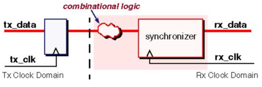
The good news is that this is relatively easy to avoid with a custom synchronizer methodology for the design and verification of clock domain crossing (CDC) logic in FPGA designs. The idea is to leverage the CDC tool to identify all the points where synchronizers need to be inserted, then put-in a more robust CDC synchronizer structure of your own creation, or from IP vendor library. Either way, the industry jargon here is that you are employing “custom sync” logic.
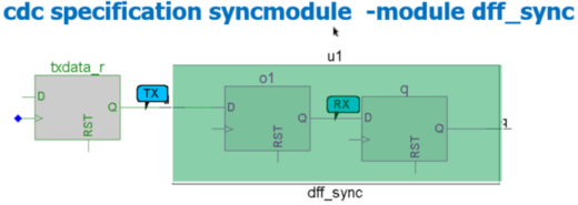
In Questa CDC, the custom synchronizer specification command (Figure 3 below) is how users can declare pre-verified synchronization structures, and also tell Questa CDC to check that this custom synchronizer is being properly used. In parallel, Questa CDC will flag manually inserted RTL-based CDC synchronizers as an error. This effectively forces the designers to use the chosen, “safer” custom sync circuitry.
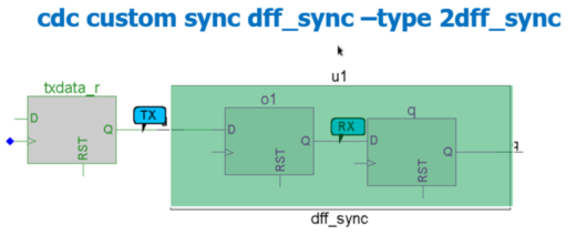
By utilizing the custom synchronizer methodology, there are 3 safeguards that can be incorporated to protect against CDC errors:
- Add protective logic into the CDC library structure
- Specify assumption checks in the custom synchronizer specification
- Declare CDC library structures as synchronizer modules
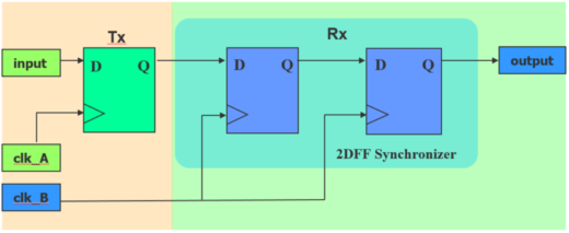
In developing a CDC synchronizer library, project teams can add these safeguards to the CDC library structures to prevent incorrect synchronizer block usage. Specifically, one technique is to include a transmit register in the library block (Figure 4 below) to avoid combinational logic violations (again, as in Figure 2 above). By adding the transmit register into the synchronizer block, this will prevent designers from adding combinational logic between the clk_A register and the 2DFF synchronizer. (Caveat: the downside of adding the protection register is that redundant registers may be included in CDC paths when designers register the data into the library synchronizer block.)
Another strategy for ensuring correct synchronizer usage is to specify safeguards when defining the custom synchronizer specification. Although designers can allow CDC tools to infer the constraints for a custom synchronizer, it is safest for designers to explicitly declare the constraints for custom synchronizers. Indeed, a complete custom synchronizer specification includes both constraints defining the internal logic as well as the external assumptions for the synchronizer block usage (Figure 5).
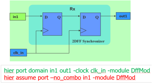
The constraints for synchronizer block include the clock domain information for the input and output ports based on the input port destination or the output port source. An important external assumption for the synchronizer block is a “no combinational logic” rule for the driving logic of an input port – it is an automatic check to see if a synchronizer is driven by combinational logic, flagging an error if this rule is violated. One advantage to this approach is that no time is wasted re-checking the pre-verified synchronizer block — only the external connections to the custom synchronizer are checked.
A third option is to add a specification constraint for the synchronizer library block. Instead of specifying the synchronizer library block as a custom synchronizer, a designer can declare the synchronizer as a designated synchronizer module (Figure 6). This designation will both check that the internal synchronizer block logic is correct as well as flag a violation when any RTL-based synchronizer structure is used. The disadvantage of this approach in comparison to the custom synchronizer approach is that the same pre-verified structure will be verified multiple times and this may impact CDC analysis performance.
With the increase in asynchronous clocks in today’s hardware designs, CDC errors are the second-leading cause of both FPGA and ASIC design re-spins [1]. Advanced CDC methodologies, such as this custom synchronizer flow, allow design teams to eliminate CDC errors.
Kurt Takara, Chris Kwok, Dominic Lucido, and Joe Hupcey III
for the Questa CDC Team
References
[1] Wilson Research Group and Mentor Graphics, “2016 Functional Verification Study”, July 2016.


Comments